Transistor Series Voltage Regulator:
When a low power zener diode is used in the simple Transistor Series Voltage Regulator, the load current is limited by the maximum diode current. A high-power Zener used in such a circuit can supply higher levels of load current, but much power is wasted when the load is light. The emitter follower regulator shown in Fig. 17-1 is an improvement on the simple regulator circuit because it draws a large current from the supply only when required by the load. In Fig. 17-1(a), the circuit is drawn in the form of the common collector amplifier (emitter follower). In Fig. 17-1(b), the circuit is shown in the form usually referred to as a series regulator. Transistor Q1 is termed a series pass transistor voltage regulator.
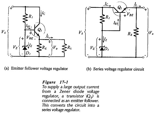
The output voltage (Vo) from the series regulator is (VZ – VBE), and the maximum load current (IL(max)) can be the maximum emitter current that Q1 is capable of passing. For a 2N3055 transistor, IL could approach 15 A. When IL is zero, the current drawn from the supply is approximately (IZ + IC(min)), where IC(min) is the minimum collector current to keep Q1 operational. The Zener diode circuit (R1 and D1) has to supply only the base current of the transistor. The Transistor Series Voltage Regulator is, therefore, much more efficient than a simple Zener diode regulator.
Series Voltage Regulator with Error Amplifier:
A series regulator using an additional transistor as an Error Amplifier is shown in Fig. 17-2. The error amplifier improves the line and load regulation of the circuit. The amplifier also makes it possible to have an output voltage greater than the Zener diode voltage. Resistor R2 and diode D1 are the Zener diode reference source. Transistor Q2 and its associated components constitute the error amplifier, that controls the series-pass transistor (Q1). The output voltage is divided by resistors R3 and R4, and compared to the Zener voltage level (V2). C1 is a large-value capacitor, usually 50 μF to 100 μF, connected at the output to suppress any tendency of the regulator to oscillate.
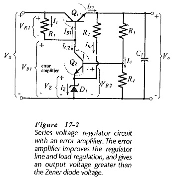
When the circuit output voltage changes, the change is amplified by transistor Q2 and fed back to the base of Q1 to correct the output voltage level. Suppose that the circuit is designed for Vo = 12 V, and that the supply voltage is VS = 18 V. A suitable Zener diode voltage in this case might be VZ = 6 V. For this VZ level, the base voltage of Q2 must be, VB2 = VZ + VBE2 = 6.7 V. So, resistors R3 and R4 are selected to give VB2 = 6.7 V and Vo = 12 V. The voltage at the base of Q1 is, VB1 = Vo + VBE1 = 12.7 V. Also, VR1 = VS – VB1 = 5.3 V. The current through R1 is largely the collector current of Q2.
Now suppose the output voltage drops slightly for some reason. When Vo decreases, VB2 decreases. Because the emitter voltage of Q2 is held at VZ, any decrease in VB2 appears across the base-emitter of Q2. A reduction in VBE2 causes IC2 to be reduced. When IC2 falls, VR1 is reduced, and the voltage at the base of Q1 rises (VB1 = VS – VR1) causing the output voltage to increase. Thus, a decrease in Vo produces a feedback effect which causes Vo to increase back toward its normal level. Taking the same approach, a rise in Vo above its normal level produces a feedback effect which pushes Vo down again toward its normal level.
When the input voltage changes, the voltage across resistor R1 changes in order to keep the output constant. This change in VR1 is produced by a change in IC2, which itself is produced by a small change in Vo. Therefore, a supply voltage change (ΔVS) produces a small output voltage change (ΔVo). The relationship between ΔVS and ΔVo depends upon the amplification of the error amplifier. Similarly, when the load current (IL) changes, IB1 alters as necessary to increase or decrease IE1. The IB1 variation is produced by a change in IC2 which, once again, is the result of an output voltage variation ΔVo.
Series Voltage Regulator without Error Amplifier:
The performance of a series regulator without an error amplifier (Fig. 17-1) is similar to that of a Zener diode regulator, except in the case of the load effect. The series-pass transistor tends to improve the regulator load effect by a factor equal to the transistor hFE.
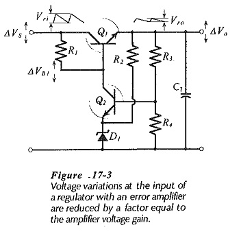
The error amplifier in the regulator in Fig 17-3 (reproduced from Fig. 17-2) improves all aspects of the circuit performance by an an amount directly related to the amplifier voltage gain (Av). When VS changes by ΔVS, the output change is,
If ΔVS is produced by a variation in the ac supply voltage, the power supply source effect is reduced by a factor of Av. ΔVS might also be the result of an increase or decrease in load current that causes a change in the average level of the dc supply voltage. Thus, the load effect of the power supply is reduced by a factor of Av.
Now consider the effect of supply voltage ripple on the circuit in Fig. 17-3. The ripple waveform appears at the collector of transistor Q1. If there was no negative feedback, it would also be present at Q1 base and at the regulator output. However, like supply voltage changes, the input ripple is reduced by a factor of Av when it appears at the output. The ripple rejection ratio is calculated as the decibel ratio of the input and output ripple voltages.
Regulator Design:
To design a Transistor Series Regulator Circuit Diagram (as in Fig. 17-3), the Zener diode is selected to have VZ less than the output voltage. A Zener diode voltage approximately equal to 0.75 Vo is usually suitable. Appropriate current levels are chosen for each resistor, and the resistor values are calculated using Ohm’s law. Transistor Q1 is selected to pass the required load current and to survive the necessary power dissipation. A heat sink (see Section 8-8) is normally required for the series-pass transistor in a regulator that supplies large load currents. As discussed, a large capacitor is usually connected across the output to ensure amplifier ac stability, (C1 in Fig. 17-3).
The difference between the regulator input and output voltages is the collector emitter voltage of the series-pass transistor (Q1), and this voltage must be large enough to keep the transistor operational. The minimum level of VCE1 (known as the dropout voltage) occurs at the lowest point in the ripple waveform of (rectified and filtered) raw dc input. If VCE1 is too small for correct operation at this point, a large-amplitude ripple waveform appears at the regulator output.