Zener Diode Voltage Regulator Circuit:
Regulator Circuit With No Load – The most important application of Zener Diode Voltage Regulator Circuit is dc voltage regulator circuits. These can be the simple regulator circuit shown in Fig. 3-19, or the more complex regulators.
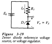
The circuit in Fig. 3-19 is usually employed as a voltage reference source that supplies only a very low current (much lower than IZ) to the output. Resistor R1 in Fig. 3-19 limits the Zener diode current to the desired level.
The Zener current may be just greater than the diode knee current (IZK). However, for the most stable reference voltage, IZ should be selected as IZT (the specified test current).
Loaded Regulator:
When a Zener diode regulator is required to supply a load current (IL), as shown in Fig. 3-21, the total supply current (flowing through resistor R1) is the sum of IL and IZ Care must be taken to ensure that the minimum Zener diode current is large enough to keep the diode in reverse breakdown.
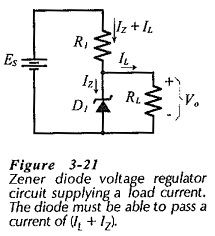
Typically, IZ(min) = 5 mA for a Zener diode with IZT = 20 mA. The circuit current equation is,
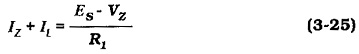
In some cases, the load current in the type of circuit shown in Fig. 3-21 may be reduced to zero. Because the voltage drop across R1 remains constant, the supply current remains constant at,
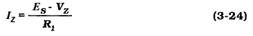
![]()
All of this current flows through the Zener diode when RL is disconnected. The circuit design must ensure that the total current does not exceed the maximum Zener diode current.
Regulator Performance:
The performance of a Zener diode voltage regulator may be expressed in terms of the source and load effects, and the line and load regulations. Equations 320 through 3-23 may be applied. If there is an input ripple voltage, the output ripple will be severely attenuated. The ripple rejection ratio is the ratio of the output to input ripple amplitudes.
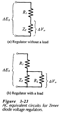
To assess the performance of a Zener diode voltage regulator, the ac equivalent circuit is first drawn by replacing the diode with its dynamic impedance (Zz), as shown in Fig. 3-23(a). The complete ac equivalent circuit is seen to be a simple voltage divider. When the input voltage changes by ΔEs, the output voltage change is,
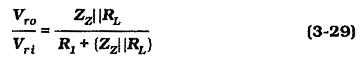
Equation 3-26 assumes that there Is no load connected to the regulator output. When a load is present, RL appears in parallel with ZZ in the ac equivalent circuit, [see Fig. 3-23(b)]. The equation for the output voltage change now becomes,
The regulator source effect can be determined from Eq. 3-26 or Eq. 3-27, as appropriate. The equations can also be used for calculating ripple rejection ratio. The input ripple amplitude (Vri ) and the output ripple (Vro) are substituted in place of the input and output voltages in Eq. 3-26 and Eq. 3-27. Thus, Eq. 3-26 can be modified to give a ripple rejection ratio equation,
and for a loaded regulator, Eq. 3-27 gives,
To determine the load effect of the Zener diode voltage regulator, the circuit output resistance has to be calculated.
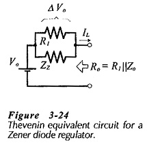
The regulator Thevenin equivalent circuit in Fig. 3-24 shows that, assuming a zero source resistance, the circuit output resistance is,
![]()
When the load current changes by ΔIL, the output voltage change is,
![]()