Zener Diode Application:
Zener diodes have numerous applications in transistor circuitry. Some of their common Zener Diode Application are explained below.
1. Zener Diode as a Voltage Regulator: Voltage regulation is a measure of a circuit’s ability to maintain a constant output voltage even when either input voltage or load current varies.
Figure 8.9 shows how a zener diode can be used as a voltage regulator to provide a constant voltage from a source whose voltage may vary appreciably. A resistor RS is necessary to limit the reverse current through the diode to safer value. The voltage source VS and the resistor RS are so selected that the diode operates in the breakdown region. The diode voltage in this region, which is also the voltage across the load RL, is called zener voltage VZ and the diode current is called the zener current IZ. The series resistor RS absorbs the output voltage fluctuations so as to maintain voltage across the load constant. Zener diode is reverse connected across the input voltage whose variations are to be regulated.
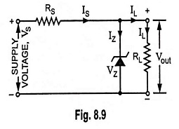
As long as voltage across the load resistor RL is less than the breakdown voltage VZ, the zener diode does not conduct, the resistors RS and RL constitute a potential divider across VS. At an increased supply voltage VS, the voltage drop across load resistor (or zener diode) becomes greater than the zener breakdown voltage. It then operates in its breakdown region. The series resistor RS limits the zener current IZ from exceeding its rated maximum IZmax. Current through resistor RS is given as
The current from the power supply splits at the junction of zener diode and the load resistor RL.
So
![]()
When the zener diode operates in its breakdown region, the voltage across it, VZ remains fairly constant even though the current IZ flowing through it may vary considerably.
When the supply voltage VS increases, the current through both the zener diode and load resistance RL increases. At the same time, however, the zener diode resistance decreases and the current through the diode increases more than proportionately. As a result, a greater voltage drop will occur across the series resistor RS and the output voltage Vout (voltage across the diode or load resistance RL) will become very close to the original value. The reverse is also true. Thus a zener diode can maintain the output voltage Vout within a fraction of a volt when the supply or input voltage VS may vary over a range of several volts. The zener diode will maintain a constant voltage across the load as long as the supply voltage is more than the zener voltage.
Let us examine the other cause of the output voltage variation. When the load resistance RL decreases for constant input voltage VS, load current IL increases. This additional current is not supplied from the source of supply but the demand of additional load current is met by decrease in zener current IZ. This keeps the voltage drop across series resistance RS constant and so the output voltage Vout. The worst case occurs for minimum source voltage and maximum load current because the zener current reduces to a minimum. In such a case,
From Eq. (8.3)
![]()
In worst case, this may be written as
![]()
The critical point occurs when IL max = IS min. At this point, the zener current, IZ reduces to zero, and regulation is lost.
By substituting IL max for IS min in Eq. (8.4), we have
where RS max is the critical value of series resistance, VS min is the minimum source voltage, VZ is zener voltage and IL max is maximum load current.
The critical resistance, RS max is the maximum allowable series resistance. The series resistance RS must always be less than the critical value; otherwise; breakdown operation is lost, and the regulator stops its operation.
The advantages of zener diode voltage regulators over other voltage regulators are that they are smaller, lighter, more rugged and have a longer life. They are also simpler and inherently cheaper.
Such regulators have the following drawbacks :
- Their efficiency is low for heavy load currents because there is a considerable power loss in series resistor RS and the diode.
- The output voltage varies slightly due to zener impedance rZ.
- The output voltage cannot be chosen independently but depends upon the breakdown voltage of the zener diode.
This regulator is employed when there are small variations in load current and supply voltage.
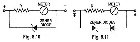
2. Meter Protection: Figure 8.10 shows how does a zener diode protect a meter (AVO meter or multimeter) movement or circuit against damage from an accidental application of excessive voltage. In this arrangement zener diode is connected in parallel with the meter. as shown in Fig. 8.10. In case of accidental overload most of the current will pass through the zener diode and so the meter movement will be saved from damage. Two zener diodes connected, as shown in Fig. 8.11, can provide overload protection regardless of the applied polarity.
3. Zener Diode as a Peak Clipper: Zener Diode Application can be used for clipping off the input waveform in waveshaping circuits, as illustrated in Fig. 8.12.
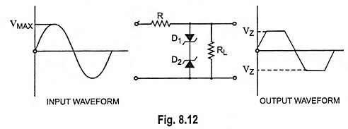
Two similar zener diodes D1 and D2 are shunted across the input sinusoidal voltage of peak value of Vmax volts. Let the zener voltage of each of zener diodes be VZ volts (VZ being lesser than Vmax).
We have seen that a zener diode acts like a ‘short’ (or very low resistance) when forward biased and ‘open’ (or very high resistance) when reverse biased till it goes into breakdown at VZ. The action of the circuit is explained below.
For positive input half cycle diode D1 is forward biased and acts like a ‘short’ while diode D2 acts like an open (being reverse biased) up to VZ. Thereafter diode D2 goes into breakdown and holds the output voltage constant at VZ till input voltage falls below VZ in the latter part of the positive half cycle. This is because during this duration of time both of the diodes act as ‘short’. When the supply voltage falls below VZ, diode D2 comes out of the breakdown and again acts as an open across the load circuit. During the negative input half cycle, the actions of diodes D1 and D2 are reversed. The result is that the output voltage waveform is clipped off on both peaks, as illustrated in Fig. 8.12.
4. Switching Operation: Zener diode can produce a sudden change from low current to high current, so it is useful for switching operations. The use of Zener Diode Application in switching operations has made possible an extremely fast performance in computer applications.
5. Zener Diode as a Reference Element: There are many applications in which it is desirable that a constant voltage is maintained between two points in a circuit, and use this voltage as reference for comparing other voltages against it. The difference between the two voltages (the voltage under comparison and reference voltage) is usually amplified and then used to perform some control function. Such an arrangement is employed in power supply voltage regulator circuits, measurement circuits and servomechanism circuits. The constant voltage characteristic of a zener diode in its breakdown region makes it desirable for such an application.
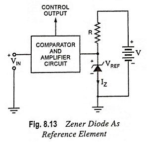
A circuit employing zener diode as a reference element is given in Fig. 8.13. The value of R is so chosen that the diode operates well within its breakdown region. VREF equals the zener breakdown voltage VZ. The difference of input voltage Vin and reference voltage VREF (i.e., Vin – VREF) provides the control output. Obviously Vin should be more than VREF.