Metal Semiconductor Junctions:
Metal semiconductor junctions are very common in all semiconductor devices and are very important. Depending upon the doping concentration, materials, and the characteristics of the interface, the metal semiconductor junctions can act as either an ohmic contact or as a Schottky barrier.
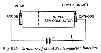
Structure of Metal Semiconductor Junctions:
A metal-semiconductor junction, as its name indicates, consists of a metal in contact with a piece of semiconductor, as shown in Fig. 6.49. The active junction is the interface between the metal, which acts as an anode, and the semiconductor. The other interface between the semiconductor and the metal, which acts as a cathode, is an ohmic contact and there is no potential drop at this junction.
Ohmic Contacts:
An ohmic contact may be defined as a metal-semiconductor contact that has a negligible contact resistance compared with the bulk or spreading resistance of the semiconductor. A satisfactory ohmic contact should not significantly perturb device performance, and it can supply the required current with a voltage drop that is considerably small compared with the drop across the active region of the device. Ideally, the current through the ohmic contact is a linear function of applied voltage, and the applied voltage should be very small.
Bulk Resistance:
After overcoming the barrier potential (or offset voltage), all that impedes the diode current is the resistance of the P and N regions, symbolized by the rP and rN in Fig. 6.50, if ohmic contact resistance is neglected. The sum of these resistances is called the bulk resistance rB of the diode i.e.,
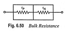
The bulk resistance of the diode depends upon the doping level, and the size of the P and N regions. Typically, the bulk resistance of rectifier diode is less than 1 Ω.
Volt–Ampere Characteristics of P–N Junction:
The graph plotted between the potential difference across the P-N junction and the circuit current is known as volt-ampere characteristic of a P-N junction.
1. Forward Characteristics: When the external voltage is zero i.e., when the circuit is open, the potential barrier at the junction does not allow the flow of current and, therefore, the circuit current is zero, as shown in Fig. 6.51.
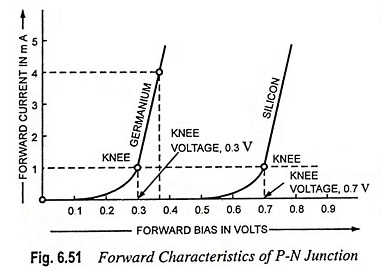
With forward bias to the P-N junction (i.e., P-region connected to +ve terminal and N-region connected to -ve terminal of the battery) very little current, called the forward current, flows until the forward voltage exceeds the junction barrier potential (0.3 V for Ge and 0.7 V for Si). The characteristics follow an exponential law. As the forward voltage is increased to the knee of the characteristic, the barrier potential is progressively reduced to zero, allowing more and more majority charge carriers to flow across the junction. Beyond the knee of the characteristic, the potential barrier is completely eliminated, forward current increases almost linearly with the increase in forward voltage and the P-N junction starts behaving as a resistor. If the forward voltage is increased beyond a certain value, extremely large current will flow and the P-N junction may get destroyed due to overheating.
Because of the nonlinear knee of the curve, if a very small signal voltage is applied to the diode so that it only operates around the knee, the signal will be distorted. The signal must, therefore, be large enough to operate the diode over the linear part of the characteristic. Forward resistance of P-N junction is low (of the order of 75 Ω in case of Ge and 150 Ω in case of Si).
2. Reverse Characteristics: When a reverse bias is applied (i.e., when P-region is connected to the negative bias terminal and N-region is connected to the positive bias terminal), as shown in Fig. 6.47(a), the potential barrier at junction is increased, therefore, the junction resistance becomes very high and there is no possibility of majority carriers flowing across a reverse biased junction. But minority carriers generated on each side can still cross the junction. Electrons on the P-side are attracted across the junction to the positive bias terminal on the N-side and holes on the N-side may travel across the junction to the negative bias terminal on the P-side. This results in a very small current, as illustrated in Fig. 6.52. This current is called reverse current and is due to minority carriers.
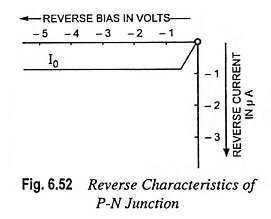
For silicon the reverse current is typically less than 1 μA and may be as low as 1 nA. In case of germanium, the reverse current may exceed 10 μA. Only a very small reverse voltage is necessary to direct all available minority carriers across the junction, and when all minority carriers are flowing across, further increase in bias voltage will not increase the current. This current is referred to as a reverse saturation current and is designated as I0. Reverse resistance is very high (of the order of MΩ).
As discussed above, the reverse saturation current I0 is made up of minority charge carriers crossing the junction. When the temperature of the semiconductor material is increased, the additional thermal energy causes more electrons to break away from atoms. This creates more hole-electron pairs and generates more minority charge carders. So reverse saturation current I0 increases with the increase in the junction temperature. It has been found that I0 approximately doubles for each 10°C rise in temperature in case of germanium and for each 8°C rise in temperature in case of silicon
Important Terms Often Used in P-N Junction:
- Breakdown Voltage: Under normal reverse voltage, a very little reverse current flows through a P-N junction. However, on increasing the reverse voltage, a point may reach at which the junction breaks down with a sudden rise in reverse current. Breakdown voltage is defined as the reverse voltage at which P-N junction breaks down with a sudden rise in reverse current.
- Knee Voltage: As already explained, with forward bias to P-N junction very little current flows until the forward voltage exceeds the junction barrier potential (0.3 V in case of Ge and 0.7 V in case of Si). The forward voltage, at which the current through the junction starts increasing rapidly, is called the knee voltage or the cutin voltage. Knee voltage of silicon diode may be defined as VK = 0.7 V. Though the lower knee voltage is an advantage and account for the use of germanium diode in certain applications, but germanium diodes are rarely used in new designs because silicon diodes have, in general, higher peak inverse voltage (PIV) and current ratings and wider temperature ranges than germanium diode.
- Maximum Forward Current: It is the highest instantaneous forward current that a P-N junction can conduct without damage to the junction. In case the forward current exceeds this rating, the junction will get destroyed due to overheating.
- Peak Inverse Voltage: It is the maximum reverse voltage that can be applied to the P-N junction without damage to the junction. If the reverse voltage across the junction exceeds its peak inverse voltage (PIV), the junction may get destroyed owing to excessive heat.
- Maximum Power Rating: It is the maximum power that can be dissipated at the junction without any damage to it.
Power dissipation for a diode can be computed in the same way as in case of a resistor. It is equal to the product of diode voltage and current i.e.,
![]()
The power rating, which is defined as the maximum power the diode can safely dissipate without shortening its life or degrading its properties, may be given as
![]()
where Vmax is the voltage corresponding to Imax. For example, if a diode has a maximum voltage of 2 V corresponding to Imax of 2.5 A, its power rating is 2 x 2.5 = 5 W.
Note: Every P-N junction has limiting values of maximum forward current, peak inverse voltage and maximum power rating. The P-N junction gives satisfactory performance when operated within these limiting values. The P-N junction may get destroyed due to excessive heat if any of these values is exceeded.