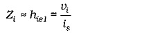
Parallel Current Negative Feedback Circuit:
Current Feedback Circuit – In series-voltage feedback, a portion of the output voltage is fed back in series with the signal source. In Parallel Current Negative Feedback Circuit, a portion of the output current is fed back in parallel with the signal source. Just as series voltage feedback stabilizes the voltage gain of a circuit, so parallel current feedback stabilizes the current gain.
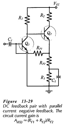
Consider the do feedback pair circuit in Fig. 13-29. An unbypassed resistor (RF2) is connected in the emitter circuit of transistor Q2, and Q1 bias resistor (RF1) is connected at the emitter terminal of Q2. With this arrangement, any ac voltage developed across RF2 is applied to RF1.
Look at the instantaneous polarities of the input voltage (vi) and feedback voltage (vf), as illustrated in the ac equivalent circuit in Fig. 13-30. When vi is moving in a positive direction, vc1 is negative-going. Because the emitter of Q2 follows the voltage (vc1) at its base, vf (across RF2) is also negative-going at this time.
Now look at the instantaneous ac current directions indicated in Fig. 13-30. When vi goes positive, the signal current (is) flows into the circuit, and an input current (ii) flows into the base of Q1, as shown. Because vf goes negative when vf is positive-going, a feedback current (if) flows in RF1 in the direction indicated, (from Q1 base toward Q2 emitter). Thus, some of the signal current is diverted away from the base of Q1. This means that the output current (ic2) is less than it would be if there was no current feedback, consequently, the circuit current gain is reduced.
Current Gain:
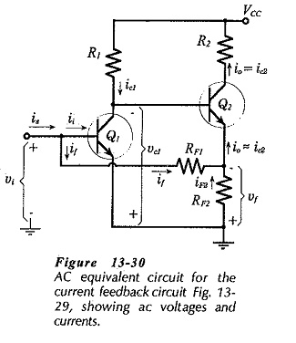
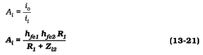
To determine the effect of negative feedback on the circuit current gain, first investigate the current gain without feedback, (the open-loop current gain). Suppose that RF2 in Fig. 13-30 has a bypass capacitor connected across it, so that there is no negative feedback. Assuming that the resistance of RF1 is very much larger than the Q1 input impedance (hie1), virtually all of is enters the base of Q1, (see Fig. 13-30).
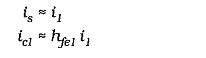
ic1 divides between R1 and Zi2. Using the current divider equation,
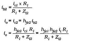
The open-loop current gain is,
Now derive an equation for the current gain with negative feedback. Referring to Fig. 13-30, it is seen that io (in the emitter circuit of Q2) divides between RF1 and RF2, giving
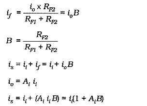
The closed-loop current gain is,
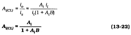
If AiB ≫ 1, then
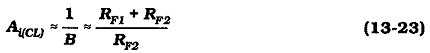
It is seen that,
Parallel Current Negative Feedback Circuit stabilizes circuit current gain.
It should be noted that, in the current gain equations, the ac output current is taken as the current in the collector circuit of transistor Q2. How this current divides between a capacitor-coupled external load (RL) and the Q2 collector resistor (R3) depends on the values of RL and R3.
Output and Input Impedances:
In the circuit shown in Figs. 13-29 and 13-30, the Q2 collector resistor (R2) is outside the feedback loop. Therefore, like the case of emitter current feedback, the output impedance of this circuit is largely unaffected by feedback. (It can be shown that the impedance looking into the collector of Q2 is increased by current feedback.) So, the circuit output impedance is, ![]()
Assuming that RF1 ≫ hie1, the circuit input impedance without feedback is,
As already shown, with negative feedback,
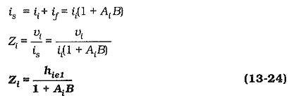
Therefore,
parallel current negative feedback reduces circuit input impedance by a factor of (1 + AiB).
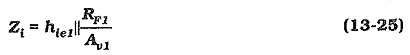
Although RF1 is a bias resistor, it is also part of the feedback network, so it is not in parallel with the circuit input impedance.
Another way of looking at the circuit input impedance is in terms of the the feedback resistor RF1 and the voltage gain of the first stage. It can be shown that,
Circuit Design:
As with other negative feedback circuits, design of a Parallel Current Negative Feedback Circuit is approached by first ignoring the ac negative feedback components. Resistors RF2 and R5 in Fig. 13-29 are calculated as a single emitter resistor (RE = RF2 + R5) to fulfill the desired dc conditions. Also, RF1 is calculated (as for other dc feedback bias circuits) to provide the required base current to Q1. RF2 is then calculated from Eq. 13-23. Usually, the resistance of RF1 is very large, and this results in a calculated resistance for RF2 larger than (RF2 + R5). In this case, the base resistor for Q1 should be made up of two resistors one of which is bypassed; see (R2 = RF1 + R7) in Fig. 13-31. RF1 is the unbypassed portion of R2, and this is calculated in relation to RF2.
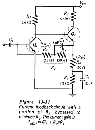
Bypass capacitor C2 (in Fig. 13-31) is calculated to give XC2 = RF2 at the desired lower cutoff frequency. Because the signal is derived from a current source, the impedance of the input coupling capacitor (C1) at f1 should be much smaller than the (normally-high) impedance of the signal source. Capacitor C3 is determined by making XC3 very much smaller than RF1 at f1.