FET and BJT Difference:
FET and BJT Difference (CS, CD, and CG Circuit Comparison) – Table 11-1 compares Zi, Zo and Av for CS, CD, and CG circuits. As already discussed, the CS circuit has voltage gain, high input impedance, high output impedance, and a 180° phase shift from input to output. The CD circuit has high input impedance, low output impedance, a voltage gain of approximately 1, and no phase shift. The CG circuit offers low input impedance, high output impedance, voltage gain, and no phase shift. 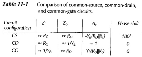
Impedance at the FET Gate:
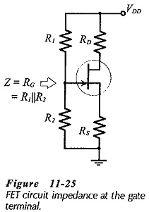
Consideration of each type of circuit shows that the input or output impedance depends upon which device terminal is involved. In both the CS and CD circuits, the input signal is applied to the FET gate terminal, so Zi is the impedance looking into the gate. Figure 11-25 shows that, for CS and CD circuits the gate input impedance is,
![]()
and the circuit input impedance is,
![]()
where RG is the equivalent resistance of the bias resistors. Because the reverse-biased gate-source resistance (Rgs) is so large, an unbypassed source resistor has no significant effect on Zi at the gate. The circuit input impedance is largely determined by RG in both the CS and CD circuits.
Impedance at the FET Source:
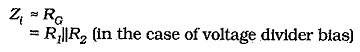
The FET source is the output terminal for a CD circuit and the input terminal for a CG circuit. The device impedance in each case is the impedance looking into the source, (see Fig. 11-26).
![]()
The circuit impedance at the source terminal must include the source resistor.
![]()
Impedance at the FET Drain:
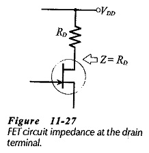
The output for CS and CG circuits is produced at the FET drain terminal. So, the impedance looking into the drain is the device output impedance (rd). As illustrated in Fig. 11-27, the circuit output impedance for any circuit with the output taken from the FET drain terminal is,
![]()
Voltage gain:
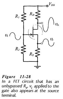
In a circuit with an unbypassed source resistor, the ac voltage at the source terminal follows the ac input at the gate, (see Fig. 11-28). A CD circuit (a source follower) has a voltage gain of approximately 1. A CS circuit with an unbypassed source resistor has vi developed across RS, and so,

In a CG circuit, and in a CS circuit with RS bypassed, the ac input (vi) is developed across the gate-source terminals, and the ac output (vo) is produced at the drain terminal. Thus, the voltage gain is the same for CS and CG circuits with similar component values and FET parameters. The CS voltage gain, equation can be used for the CG circuit, with the omission of the minus sign that indicates CS phase inversion.
Although the voltages gains are equal for similar CS and CG circuits, the low input impedance of the CG circuit can substantially attenuate the signal voltage, and result in a low amplitude output.
FET-BJT circuit Comparison:
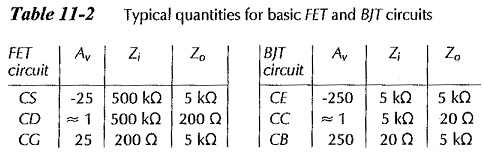
Table 11-2 compares Zi, Zo and Av for the basic FET and BJT circuits. The BJT CE and CB circuits have much higher voltage gains than the corresponding FET CS and CG circuits, while the FET CS and CD circuits have much higher input impedances than the BJT CE and CC circuits. Apart from these FET and BJT Difference, BJTs and FETs can generally perform similar functions. High-frequency, fast-switching, and high-power devices of both types are available. In some switching applications, FETs have the advantage of a smaller voltage drop (VDS(on)) than that across BJTs (VCE(sat)).