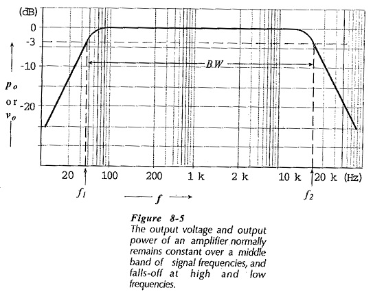
High Frequency Analysis of BJT:
Coupling and Bypass Capacitor Effects – Consider the typical High Frequency Analysis of BJT illustrated in Fig. 8-5. As discussed, the amplifier voltage gain is constant over a middle range of signal frequencies, and it falls at the low and high ends of the frequency range.
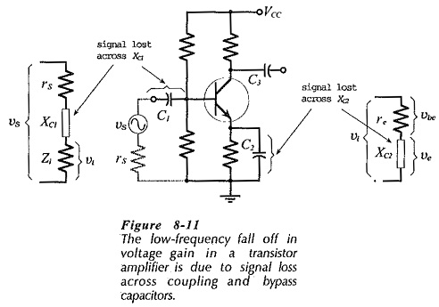
The gain fall-off at low signal frequencies is due to the effect of coupling and bypass capacitors. Recall that the reactance of a capacitor is XC = 1/(2πfC). At medium and High Frequency Analysis of BJT, the factor f makes XC very small, so that all coupling and bypass capacitors behave as ac short circuits. At low frequencies, XC is large enough to divide the voltages across the capacitors and series resistances, (see Fig. 8-11). As the signal frequency gets lower, the capacitive reactance increases, more of the signal is lost across the capacitors, and the circuit gain continues to fall.
High Frequency Analysis of CE Amplifier and CB Circuits:
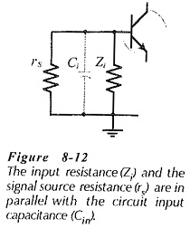
The input capacitance of an amplifier reduces the circuit gain by 3 dB when the capacitive impedance equals the resistance in parallel with the input, (see Fig. 8-12). That is when,
![]()
So, all circuits have an input capacitance limited upper cutoff frequency (f2(i)). As already explained, the input capacitance of a CE circuit is amplified by the Miller effect, but Miller effect does not occur in a CB circuit. Consequently, a CB circuit operates to a much higher signal frequency than a similar CE circuit.
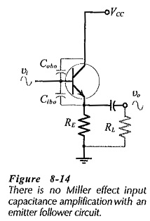
Input Capacitance Effects on Emitter Follower:
When a High Frequency Analysis of BJT is used as an emitter follower its BE junction voltage is not significantly altered by the ac input signal, because virtually all of vi appears at the emitter as vo, (see Fig. 8-14). Also, there is no Miller effect to amplify Cbc, so the input capacitance is Cibo||Cobo. The input capacitance limited cutoff frequency for an emitter follower is very much higher than that for a CE circuit.
Stray Capacitance:
Figure 8-15 illustrates the fact that stray capacitances (Csi and Cso) exists in all High Frequency Analysis of BJT circuits. This is capacitance between connecting wires and ground, and normally it is extremely small. The stray capacitance at the device base is usually much smaller than the input capacitance at the base, so that it can normally be neglected. When this is not the case, the stray capacitance must be included with the input capacitance for CE circuit cutoff frequency calculations.
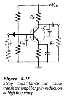
At the circuit output, the impedance of the stray capacitance (Cso) is very high at low and medium signal frequencies, so that it has no effect on the gain. At High Frequency Analysis of BJT, the stray capacitive impedance becomes small enough to shunt away some of the input and output currents, and thus it reduces the circuit gain. Referring to Fig. 8-15, it is seen that circuit ac load consists of the output stray capacitance (Cso) in parallel with RC and RL. Rewriting the voltage gain equation for CE and CB circuits,
If the transistor cutoff frequency has not caused the gain to fall off at a lower frequency, then the gain falls by 3 dB when Xcso = RC||RL. This is an output capacitance limited cutoff frequency (f2(o)).
If the voltage gain falls by 3 dB at fαe due to the transistor, and by 3 dB at the same frequency due to the stray capacitance, then the gain is down by 6 dB. Consequently, the amplifier upper cutoff frequency is lower than fαe. This is illustrated in Fig. 8-16.
As discussed, there is an additional 3 dB attenuation when Xcso = RC||RL. If Xcso = 2(RC||RL) at fαe , the additional attenuation can be shown to be 1 dB, (see Fig. 8-16). With Xcso = 5(RC||RL) at fαe , there is only 0.2 dB additional attenuation, as illustrated.
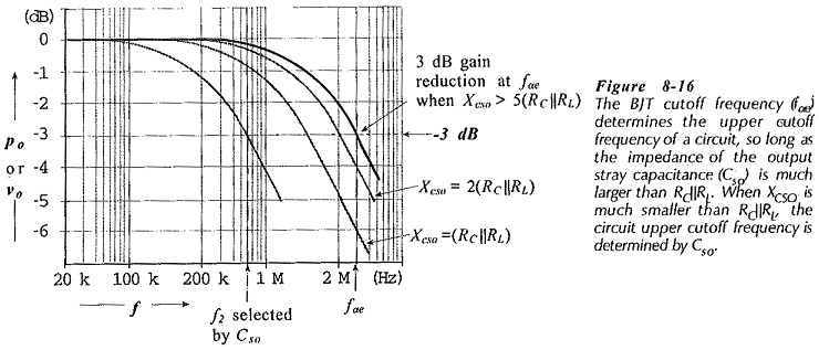
In some circumstances it is desirable to set the upper cutoff frequency of a circuit at a frequency well below the transistor cutoff frequency, (see Fig. 8-16). This is done simply by connecting a capacitor from the collector terminal to ground exactly as Cso is shown in Fig. 8-15. The capacitance value is calculated at the desired cutoff frequency to give,
![]()