Transistor Construction:
The transistor construction consists of a silicon or germanium (preferably silicon because of its smaller cutoff current ICBO, smaller variations in ICBO due to variations in temperature and higher operating temperature) crystal in which a layer of N-type material is sandwiched between two layers of P-type material, as shown in Fig. 10.1 (a).
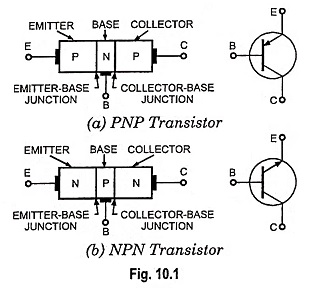
Alternatively a transistor construction may consist of a layer of P-type material sandwiched between two layers of N-type material, as shown in Fig. 10.1 (b).
In the former case the transistor is referred to as a P-N-P transistor and in latter case, as an N-P-N transistor. Each type of transistor has two P-N junctions—one junction between the emitter and base, called the emitter-base junction or simply the emitter junction and the other junction between the base and collector, called the collector-base junction or simply the collector junction.
Thus a transistor is like two P-N junction diodes connected back to back. The two junctions give rise to three regions provided with three terminals called the emitter, base and collector, as shown in Fig. 10.1. The emitter, base and collector correspond in a general way to the cathode, grid and plate or anode of a vacuum triode.