Silicon Bilateral Switch:
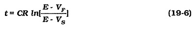
It might be convenient to think of a Silicon Bilateral Switch (SBS) as an SUS with a gate terminal, or as a low-current TRIAC. However, the SBS is not simply another four-layer device. Silicon bilateral switches are actually integrated circuits constructed of matched transistors, diodes, and resistors. This produces better parameter stability than is possible with four-layer devices. The SBS equivalent circuit in Fig. 19-31(a) is similar to the TRIAC equivalent circuit with the addition of resistors R1 and R2 and Zener diodes D1 and D2. The device circuit symbol in Fig. 19-31(b) is seen to be composed of inverse-parallel connected SUS symbols with a gate terminal added. Note that the terminals are identified as anode 1 (A1), anode 2 (A2), and gate (G). The typical Silicon Bilateral Switch characteristics shown in Fig. 19-31(c) are essentially the same shape as TRIAC characteristics.
Returning to the equivalent circuit, the SBS switches on when a positive A1A2 voltage is large enough to cause D2 to break down. This produces base current in Q1, resulting in Q1 collector current that switches Q2 on. Similarly, a negative A1A2 voltage causes D1 to break down, producing base current in Q4 that turns Q4 and Q3 on. The switching voltage is the sum of the Zener diode voltage and the transistor base-emitter voltage, (VS = VZ + VBE). The Zener diode has a positive temperature coefficient (TC) and the transistor base-emitter voltage has a negative TC. This results in a very small TC for the SBS switching voltage.
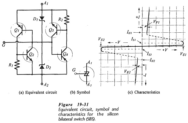
The partial specification for a MBS4991 SBS in Fig. 19-32 shows a switching voltage that ranges from 6 V to 10 V. Note also that the switching voltage differential (the difference between the switching voltages in opposite directions), (VS1 – VS2), is 0.5 V maximum. The maximum switching current is a 500 μA, and the switching current differential (IS1 – IS2) is 100 μA.
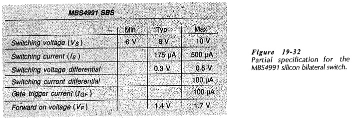
Silicon Bilateral Switch devices are frequently used with the gate , open-circuited, so that they simply breakdown to the forward voltage drop when the applied voltage increases to the switching voltage level. The switching voltage can be reduced by connecting Zener diodes with VZ lower than 6.8 V between the gate and the anodes, as shown in Fig. 19-33(a). The new switching voltage is approximately (VZ + 0.7 V). The switching voltage can also be modified by the use of external resistors, [Fig. 19-33(b)]. Taking the gate current into account, it can be shown that the two 22 kΩ resistors reduce VS to approximately 3.6 V.
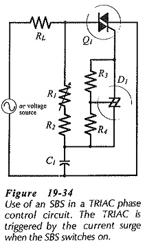
The use of an Silicon Bilateral Switch in a TRIAC phase control circuit is illustrated in Fig. 19-34. This is essentially the same as the circuit using a DIAC. The SBS turns on and triggers the TRIAC when the capacitor voltage equals the SBS switching voltage plus the TRIAC gate triggering voltage.
For an SBS to switch on, the total resistance in series with it must have a maximum value that allows the switching current to flow. If the resistance is so large that it restricts the current to a level below the SBS switching current, the device will not switch on. Also, the series resistance must not be so small that it allows the holding current to flow when the SBS is supposed to switch off These restrictions also apply to SCRs, TRIACS, DIACS, and other similar switching devices. Switch-off is usually no problem in thyristor circuits with ac supplies, because the devices normally switch off when the instantaneous supply voltage reduces to zero. With dc supplies, more care must be taken with resistor sizes.
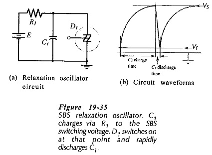
Figure 19-35 shows a simple circuit that requires careful design to ensure that the Silicon Bilateral Switch switches on and off as required. The circuit is a relaxation oscillator that produces an exponential output waveform, as illustrated. Capacitor C1 is charged via resistor R1 from the dc supply voltage (E). When the capacitor voltage (VC) reaches the SBS switching voltage (VS), D1 switches on and rapidly discharges the capacitor to the D1 forward voltage (VF). Then D1 switches off and the capacitor commences to charge again. The SBS will not switch off if the D1 holding current (IH) continues to flow through R1 when VC equals VF SBS switch-on will normally occur when VC equals VS regardless of the R1 resistance, because the capacitor discharge should provide the switching current (IS). However, it is best to select R1 small enough to allow IS to flow at D1 switch on.
The approximate oscillation frequency can be determined from the capacitor charging time (t), and the equation for t is derived from the RC charging equation.