Silicon Controlled Rectifier Principle Operation:
Silicon Controlled Rectifier Principle Operation (SCR) consists of four layers of semiconductor material, alternately p-type and n-type as illustrated in Fig. 19-1(a). Because of its construction, the SCR is sometimes referred to as a four-layer diode, or a pnpn device. The layers are designated p1,n1,p2, and n2, as shown. There are three junctions; J1, J2, and J3, and three terminals; anode (A), cathode (K), and gate (G). Figure 19-1(b) shows the Silicon Controlled Rectifier Principle Operation circuit symbol.
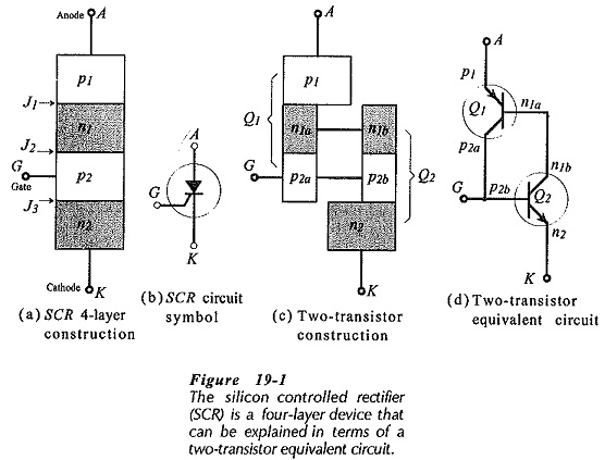
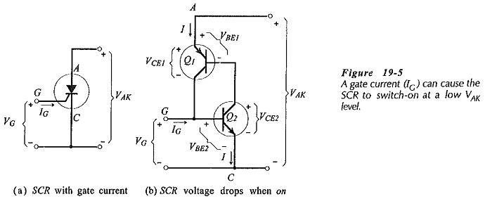
To understand Silicon Controlled Rectifier Principle Operation, it is necessary to imagine layers n1 and p2 split into n1a, n1b, P2a and P2b as shown in Fig. 19-1(c). Since n1a is connected to n1b, and P2a is connected to p2b, nothing is really changed. However, it is now possible to think of p1, n1a, P2a as a pnp transistor, and n1b, P2b, n2 as an npn transistor. Replacing the transistor block representations in Fig. 19-1(c) with the pap and npn BJT circuit symbols gives the two-transistor equivalent circuit in Fig. 19-1(d). It is seen that the Q1 collector is connected to the Q2 base, and the Q2 collector is commoned with the Q1 base. The Q1 emitter is the SCR anode terminal, the Q2 emitter is the cathode, and the junction of the Q1 collector and the Q2 base is the SCR gate terminal.
To forward bias an SCR, a voltage (VAK) is applied positive on the anode (A), negative on the cathode (K), as shown in Fig. 19-2(a). If the gate (G) is left unconnected only small leakage currents (ICO) flow, and both transistors remain off. Reference to Fig. 19-1(a) shows that the leakage currents are the result of junction J2 being reverse biased when A is positive and K is negative.
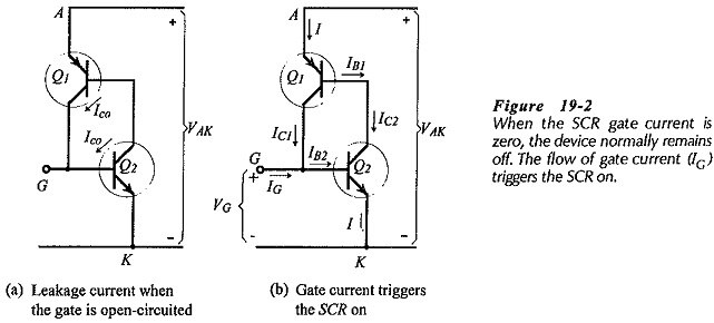
When a negative gate-cathode voltage (-VG) is applied, the Q2 base-emitter junction is reverse biased, and only small leakage currents continue to flow, so both Q1 and Q2 remain off. A positive gate-cathode voltage forward biases the Q2 base-emitter junction, causing a gate current (IG = IB2) to flow, and producing a Q2 collector current (IC2), [see Fig. 19-2(b)]. Because IC2 is the same as IB1, Q1 also switches on and IC1 flows providing base current IB2. Each collector current provides much more base current than needed by the transistors, and even when IG is switched off the transistors remain on, conducting heavily with only a small anode-to-cathode voltage drop. The ability of the SCR to remain on when the triggering current is removed is referred to as latching.
To switch the SCR on, only a brief pulse of gate current is required. Once switched on, the gate has no further control and the device remains on until VAK is reduced to near zero.
Consider Fig. 19-1(a) again. With a forward (anode-to-cathode) bias, junctions J1 and J3 are forward biased, while J2 is reverse biased. When VAK is made large enough, J2 will break down and the resultant current flow across the junction constitutes collector current in each transistor. Each collector current flows into the base of the other transistor causing both transistors to switch on. Thus, the SCR can be triggered on with the gate open-circuited.
SCR Characteristics and Parameters:
Figure 19-3(a) shows an Silicon Controlled Rectifier Principle Operation with a reverse bias anode-to-cathode voltage (- VAK), (negative on A, positive on K). Note that the gate terminal is open-circuited. Figure 19-3(b) shows that the reverse bias voltage causes junction J2 to be forward biased and J1 and J3 to be reverse biased. When -VAK is small, a reverse leakage current (IRX) flows. This is plotted as the reverse characteristic (-VAK versus IR) on Fig. 19-3(c). IRX is typically around 100 μA, and is sometimes referred to as the reverse blocking current.
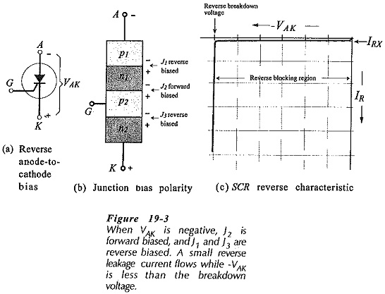
When the level of -VAK is increased, IRK remains approximately constant until the reverse breakdown voltage is reached. At this point the reverse-biased junctions (J1 and J3) break down and the reverse current (IR) increases very rapidly. If IR is not limited (by additional circuit components) the device will be destroyed by excessive current flow. The region of the reverse characteristics before breakdown is termed the reverse blocking region.
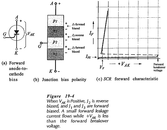
An SCR with a forward bias anode-to-cathode voltage (positive on A, negative on K) is shown in Fig. 19-4(a). Here again, the gate terminal is open-circuited. As illustrated in Fig. 19-4(b), +VAK forward biases J1 and J3 and reverse biases J2. With low levels of +VAK, a small forward leakage current (IFX) flows. This is actually the reverse leakage current at junction (J2), and so (like IRK), it is typically around 100 μA Also like IRK, IFX remains substantially constant until +VAK is made large enough to cause (reverse biased) J2 to break down. The applied voltage at this point is termed the forward breakover voltage (VF(BO)). This is illustrated by the forward characteristics (IF versus +VAK) in Fig. 19-4(c). When VF(BO) is reached, the component transistors (Q1 and Q2) are immediately switched on into saturation as already explained, and the anode-to-cathode voltage falls rapidly to the forward conduction voltage VF The device is now into the forward conduction region, and IF must be limited to protect the SCR from excessive current levels.
So far, me SCR forward characteristics have been discussed only for the case of IG = 0. Now consider the effect of IG levels greater than zero, wig. 19-5(a)1. As already shown, when +VAK is less than VF(BO)) and IG is zero, a small leakage current flows. This current is too small to have any effect on the level of +VAK that causes SCR switch on. When IG is made just slightly larger than the junction leakage currents, it still has a negligible effect on the level of +VAK for switch-on. Now consider the opposite extreme. When IG is made larger than the minimum base current required to switch Q2 on, the SCR switches-on when +VAK forward biases the base-emitter junctions of Q1 and Q2, [Fig. 19-5(b) and Fig. 19-6].
The complete forward characteristics for an Silicon Controlled Rectifier Principle Operation are shown in Fig. 19-6. Note that when IG = IG4 switch-on occurs with +VAK at a relatively low level (V4). Gate currents between IGO and IG4 device switch-on at voltages greater than V4 and less than VF(BO). The region of the forward characteristics before switch-on occurs is known as the forward blocking region, and the region after switch-on is termed the forward conduction region, as illustrated. In the forward conduction region, the SCR behaves as a forward-biased rectifier. The forward (anode-to-cathode) voltage (VF) when the device is on is typically 1.7 V.
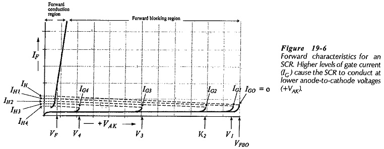
To switch an SCR of the forward current (IF) must be reduced below the holding current (IH), (see Fig. 19-6). The holding current is the minimum level of IF that maintains SCR conduction. If a gate current greater than zero is maintained while the SCR is on, lower levels of holding current (IH1, IH2, etc.,) are possible.
SCR Specification:
As in the case of most electronic devices, the SCR maximum voltage and current are important for any given application. The forward breakover voltage and reverse breakdown voltage have already been discussed. The maximum forward voltage that may be applied without causing the SCR to conduct is termed the forward blocking voltage (VDRM). Similarly, the maximum reverse voltage that may be applied is the reverse blocking voltage (VRRM).
The maximum SCR current is variously specified as: the average current (IT(AV)), the rms cunerit (IT(RMS)), and the peak non-repetitive surge current (ITSM). The first two of these need no explanation. The third is a relatively large current that can normally be permitted to flow for a maximum of a half-cycle of a 60 Hz sine wave. The circuit fusing rating (I2t) is another parameter that defines the maximum nonrepetitive forward current. This can be used to calculate the maximum time duration for a given forward current surge. In many circuit applications the SCR current is limited by a series-connected load, so there is usually no need to consider surge current levels, except in the case of capacitive loads.
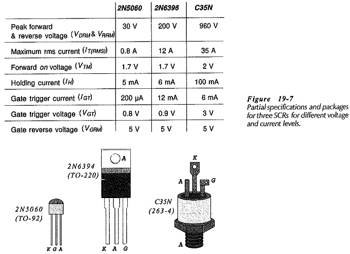
Some of the range of available SCRs is illustrated by the partial specifications and packages shown in Fig. 19-7. With 800 mA rms current and 30 V forward and reverse blocking voltage, the 2N5060 is a relatively low-current, low-voltage, device. This is packaged in the typical plastic TO-92 transistor-type enclosure. Note that the peak reverse gate voltage (VGRM) is 5 V. The 2N6396 SCR is capable of handling a maximum rms current of 12 A, and has forward and reverse blocking voltage of 200 V. The package is a TO-220 plastic enclosure with a metal tab for mounting on a heat sink. For the C35N, the peak forward and reverse voltage is 960 V, and maximum rms current is 35 A. The device package is designed for bolt-mounting to a heat sink.