Half Wave Rectifier Circuit:
A basic diode Half Wave Rectifier Circuit is shown in Fig. 3-1(a). An alternating input voltage is applied to a single diode connected in series with a load resistor RL. The diode is forward biased during the positive half-cycles of the input waveform, and reverse biased during the negative half-cycles. Substantial current flows through RL only during the positive half-cycles of the input. For the duration of the negative half-cycles, the diode behaves almost as an open switch.
The output voltage waveform developed across RL is a series of positive half-cycles of alternating voltage with intervening very small negative voltage levels produced by the diode reverse saturation current.
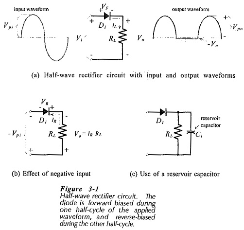
When the diode is forward biased [Fig. 3-1(a)1, the voltage drop across it is VF, and the output voltage is (input voltage) – VF. So, the peak output voltage is,
![]()
Note that Vpi= 1.414 Vi , where Vi is the rms level of the sinusoidal input voltage.
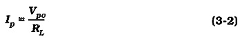
The diode peak forward current is,
During the negative half-cycle of the input [Fig. 3-1(b)], the reverse-biased diode offers a very high resistance. So, only a very small reverse current (IR) flows, giving an output voltage,
![]()
While the diode is reverse biased, the peak voltage of the negative half-cycle of the input is applied to its terminals. Thus, the peak reverse voltage, or peak inverse voltage (PIV), applied to the diode is,
![]()
Most Half Wave Rectifier Circuit use a reservoir capacitor at the output terminals to smooth the rectified voltage wave into direct voltage [see Fig. 3-1(c)l. It is important to note that the presence of the reservoir capacitor substantially changes the rectified voltage waveform and affects the diode current and voltage requirements.