JFET Characteristics:
An n-channel JFET Characteristics block representation is shown in Fig. 9-6. With a drain-source voltage applied as illustrated, ID flows in the direction shown producing voltage drops along the channel. Consider the voltage drops from the source terminal (S) to points A, B. and C within the channel. Point A is positive with respect to the source: alternatively, it can be stated that S is negative with respect to A. Because the gate blocks are connected to S, the gates are negative with respect to point A by a voltage VA. This causes the depletion regions to penetrate into the channel by an amount proportional to VA.
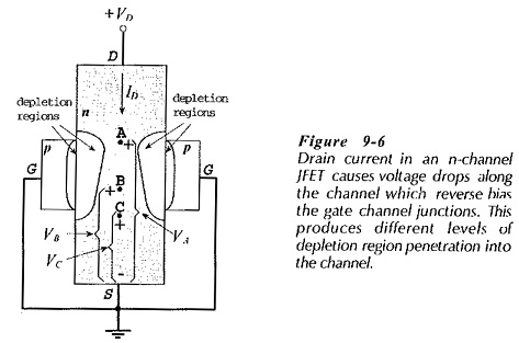
The voltage drop between point B and the source is VB, which is less than VA. Consequently, at point B on the channel the gates are at -VB with respect to the channel, and the depletion region penetration is less than at point A. From point C to the source terminal, the voltage drop (VC) is less than VB. Thus, the gate-channel reverse bias (at point C) is VC volts, and the depletion region penetration is less than at point A or B. The differing voltage drops along the channel, and the resulting variation in gate-channel reverse bias, accounts for the shape of the depletion region penetration of the channel.
Drain Characteristics of jfet with VG = 0:
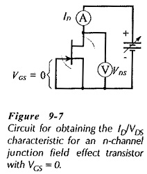
Figure 9-7 shows a circuit for determining the drain current versus drain-source voltage characteristics of n channel jfet with VGS = 0. VDS is increased in convenient steps from zero, and ID is measured at each VDS level. This produces a table of ID/VDS values for plotting the characteristic shown in Fig. 9-8.
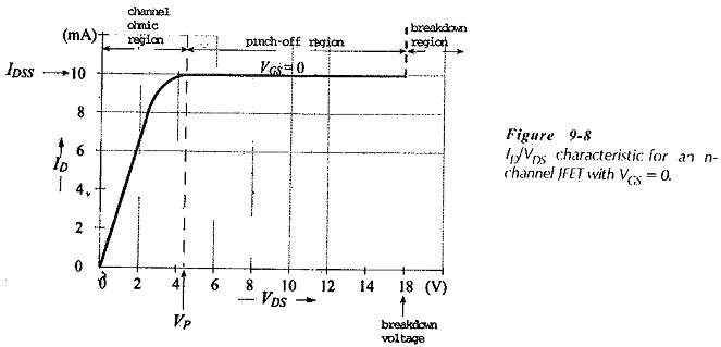
Referring to the JFET Characteristics, it is seen that when VDS = 0, ID = 0. There is no channel voltage drop, so the voltage between the gate and all points on the channel is zero, and there is no depletion region penetration. When VDS is increased by a small amount (less than 1 V), a small drain current flows producing some voltage drop along the channel. This results in some depletion penetration of the channel (as explained for Fig. 9-6), but it is so small that it has no significant effect on the channel resistance. With further small increases in VDS the drain current increase is approximately linear, and the channel behaves as an almost constant-value resistance, (see Fig. 9-8).
The channel continues to behave as a fixed-value resistance until the voltage drops along it become large enough to produce considerable depletion region penetration. At this stage the channel resistance begins to be affected by the depletion regions. Further increases in VDS now produce smaller ID increases, as shown by the curved part of the JFET Characteristics. The increased ID levels, in turn, cause more depletion region penetration and greater channel resistance. Eventually, a saturation level of ID is reached where further VDS increase seems to have no effect on ID.
At the point on the characteristic where ID levels off, the drain current is referred to as the drain-source saturation current(IDSS). (10 mA in Fig. 9-8). The shape of the depletion regions in the channel at the IDSS level is such that they appear to pinch off the channel, (see Fig. 9-6). So, the drain source voltage at this point is termed the pinch-off voltage (VP), (4.5 V in Fig. 9-8.) The region of the JFET Characteristics where ID is constant is called the pinch-off region, as illustrated. The channel mostly behaves like a resistance between VDS = 0 and VDS = VP, so this part of the characteristic is referred to as the channel ohmic region.
If VDS is continuously increased (in the pinch-off region) a voltage is reached at which the (reverse-biased) gate-channel junctions break down, (see Fig. 9-8). When this occurs, ID increases rapidly, and the device might be destroyed. The pinch-off region of the characteristic is the normal operating region for the FET.
Drain Characteristics with External Bias:
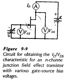
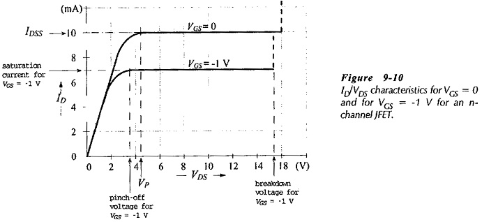
A circuit for obtaining the ID/VDS characteristics for an n-channel JFET when an external gate-source bias (VGS) is applied is shown in Fig. 9-9. In this case, VGS is set to a convenient (negative) level (such as -1 V). VDS is increased in steps, and the corresponding level of ID is noted at each VDS step. The ID/VDS characteristic for VGS = -1 V is then plotted as illustrated in Fig. 9-10.
When a -1 V external gate-source bias voltage is applied, the gate-channel junctions are reverse biased even when ID = 0. So, when VDS = 0 the depletion regions are already penetrating to some depth into the channel. Because of this, a smaller voltage drop along the channel (smaller than when VGS = 0) will increase the depletion regions to the point at which they produce channel pinch-off. Consequently, with VGS = -1 V the pinch-off voltage is reached at a lower ID level than when VGS = 0. The VGS = -1 V characteristic In Fig. 9-10 has V p = 3.5 V.
A family of drain characteristics can be obtained by using several levels of negative gate-source bias voltage, (see Fig. 9-11). If a positive VGS is used, a higher level of ID can be produced, as shown by the JFET Characteristics for VGS = +0.5 V. However, VGS is normally kept negative to avoid the possibility of forward biasing the gate-channel junctions.
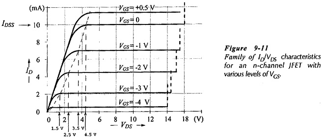
The dashed line on the characteristics in Fig. 9-11 is drawn through the points at which ID saturates for each level of gate-source bias voltage. When VGS = 0, ID saturates at IDSS, and the characteristic shows VP = 4.5 V. When a -1 V external bias is applied, the gate-channel junctions still require -4.5 V to achieve pinch-off, This means that a 3.5 V drop is now required along the channel instead of 4.5 V, and the lower voltage drop is achieved with a lower level of ID. Similarly, when VGS = -2 V and – 3 V, pinch-off is achieved with 2.5 V and 1.5 V, respectively, along the channel. The 2.5 V and 1.5 V drops are, of course, obtained with further reduced ID levels.
Suppose a -4.5 V gate-source bias is applied to a device with the JFET Characteristics shown in Fig. 9-11. This is a VGS level equal to the pinch-off voltage Vp. Without any additional channel voltage drop produced by ID, the depletion regions penetrate so deep into the channel that they meet in the middle, completely cutting ID off. So, a gate-source bias equal to the pinch-off voltage reduces ID to zero. The bias voltage required to do this is termed the gate cutoff voltage (VGS(0)). and, as explained. VGS(0) = Vp. Note on Fig. 9-11 that the drain-source voltage at which breakdown occurs is reduced as the negative gate-source bias voltage is increased. This is because -VGS adds to the reverse bias at the junctions.
Transfer Characteristics of jfet:
Transfer Characteristics of jfet are a plot of ID versus VGS. The gate-source voltage of a FET controls the level of the drain current, so, the transfer characteristic shows how ID is controlled by VGS. As illustrated in Fig. 9-13(a), the transfer characteristic extends from ID = IDSS at VGS = 0, to ID = 0 at VGS = Vp.
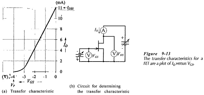
Figure 9-13(b) shows a circuit for experimentally determining a table of quantities for plotting the transfer characteristic of a given FET. The drain-source voltage is maintained constant, VGS is adjusted in convenient step, and the corresponding levels of VGS and ID are recorded. The characteristic shows that, as -VGS is increased, ID is progressively reduced from IDSS at VGS = 0, to ID = 0 at VGS = -Vp
The transfer characteristic for a FET can be derived from the drain characteristics. A line is drawn vertically on the drain characteristics to represent a constant VDS level. The corresponding ID and VGS values along this line are noted and then used to plot the transfer characteristic.
p channel jfet characteristics:
Figure 9-15 shows a circuit for obtaining the JFET Characteristics of a p-channel JFET. Note the direction of the arrowhead on the PET symbol, and the drain current direction. Also, note the supply voltage polarity, and the polarity of the gate-source bias voltage. The drain terminal is negative with respect to the source, and the gate terminal is positive with respect to the source. To obtain a table of quantities to plot a drain characteristic, VGS is maintained constant at the desired (positive) level, -VDS is increased in steps from zero, and the ID levels are noted at each step.
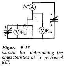
Typical p- hannel JFET drain characteristics and transfer characteristics are shown in Fig. 9-16. It is seen that these are similar to the characteristics for an n-channel JFET, except for the voltage polarities. In Fig. 9-16, when VGS = 0, IDSS = 15 mA, and progressively more positive levels of VGS reduce the level of ID toward cutoff at Vp = +6 V. Using VGS = -0.5 V produces a higher level of ID than when VGS = 0. As in the case of the n-channel JFET, forward bias at the gate-channel junctions should be avoided, consequently, negative VGS levels are normally not used with a p-channel JFET.
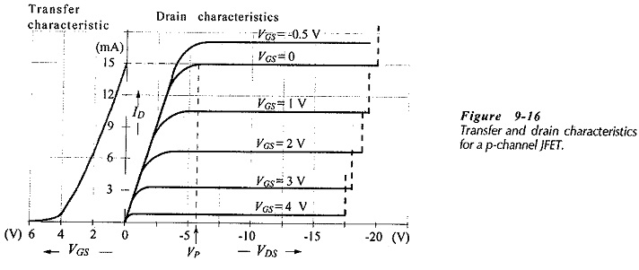
The transfer characteristics of p channel jfet device can be obtained experimentally, or can be derived from the drain characteristics, just as for an n-channel FET.