JFET Biasing Circuits:
Use of Plus/Minus Supplies – When plus/minus supply voltages are to be used with a JFET Biasing Circuits, the gate terminal is usually grounded via RG, as illustrated in Fig. 10-40(a). In this case, the circuit is essentially a voltage divider bias circuit with the gate bias voltage equal to the level of the negative supply voltage, (VG = VSS). The (reverse) gate-source bias voltage (-VGS) makes the source terminal +VGS above ground. So, ![]()
When the voltage levels are understood, the type of circuit in Fig. 10-40(a) can be designed using a procedure similar to that for a voltage divider bias circuit. ID(max) is plotted on the maximum transfer characteristics, and VGS is read from the horizontal axis VGS can also be determined by substituting ID(max), IDSS(max), and VP(max) into Eq. 10-8. Then, with the desired maximum voltage drops known, RD and RS are readily calculated. RG is selected as 1 MΩ, or less, for the reasons already discussed.
![]()
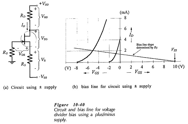
Analysis procedure for this circuit is also like that for a voltage divider bias circuit. One point on the bias line is plotted on the transfer characteristics at VG = VSS, as shown on Fig. 10-40(b), and the bias line is drawn at the slope determined by Rs. As always, the bias line intersections with the maximum and minimum characteristics gives the ID(max) and ID(min) levels.
Drain Feedback:
The drain feedback JFET Biasing Circuits in Fig. 10-41 is essentially a voltage divider bias circuit. However, instead of VG being derived from the supply voltage, the FET drain voltage (VD) is divided by R1 and R2 to produce VG. Modifying Eq. 10-7,
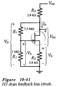
The circuit is designed for a particular level of VD and ID, and the voltage drop across RS helps to stabilize ID, as in other voltage divider bias circuits. The voltage drop across RD also provides feedback that helps to correct changes in ID. When ID is greater than the design value, VRD is increased, VD is reduced, and thus VG is lowered to drive ID back toward its original level. The two feedback effects (VRD changes and VRS changes) tend to keep ID(min) and ID(max) closer than in an ordinary voltage divider JFET Biasing Circuits.
Design procedure for this circuit is the same as for voltage divider bias with the exception that the voltage drop across R1 is (VD – VG) instead of (VDD – VG). For circuit analysis a bias line should be drawn on the transfer characteristics, as always. This requires the equation relating VGS and ID.
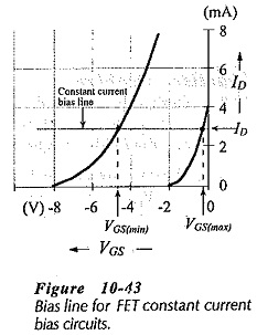
Constant Current Bias:
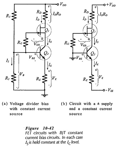
As already discussed, the bias lines with the smallest slope give the closest levels of ID(min) and ID(max). In the two circuits in Fig. 10-42 the bipolar transistor (Q2) keeps the FET source current constant. Consequently, as illustrated in Fig. 10-43, the bias line is drawn horizontally on the transfer characteristics, showing ID(min) = ID(max), with different VGS levels.
Both circuits provide bias voltage VB to the base of Q2, to give,
The circuit in Fig. 10-42(a) uses voltage divider bias to derive VB from VDD, and in Fig. 10-42(b) VB = VEE. In both cases, the FET gate is connected to the base of Q2 via resistor RG, and VGS = -VCB.
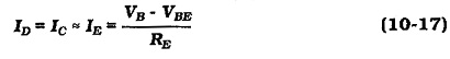
Design of each of the circuit in Fig. 10-42 simply involves selection of appropriate voltage and current levels and calculation of the resistors. The emitter resistor voltage drop (VE) should typically be a minimum of 5 V, but satisfactory results can be obtained with 3 V. It can, of course, be much larger than 5 V, as would normally be the case in Fig. 10-42(b). In both circuits,![]()
The level of VB calculated in this way can be used to determine the ratio of R1 and R2 in Fig. 10-42(a). For the circuit in Fig. 10-42(b), VEE indicates the VB and VE levels.
The maximum VGS level is determined by plotting ID on the maximum transfer characteristic for the FET, and then reading VGS(max) at ID. Alternatively, VGS can be calculated from Eq. 10-8. The source terminal voltage is more positive than the gate. The equation for VS,
![]()
Analysis of each of the circuits in Fig. 10-42 is very simple. Once VB is determined, ID is calculated using Eq. 10-17. VGS(max) and VGS(min) are found by drawing the bias line for ID on the transfer characteristics, or by substituting ID, VP, and IDSS into Eq. 10-8.