Performance of CMOS Gates:
The Performance of CMOS Gates which based on following different categories namely,
Operating Speed : Slower than TTL series. Approximately 25 to 100 ns depending on the subfamily of CMOS Inverter Circuit. It also depends on the power supply voltage.
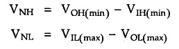
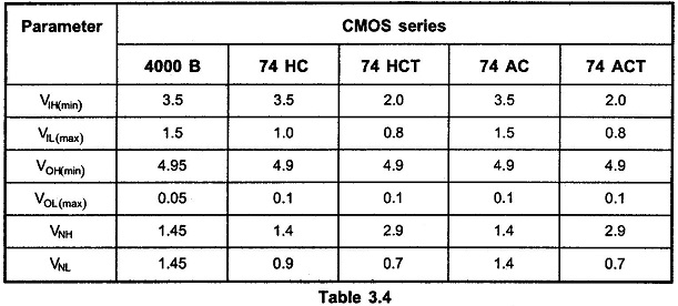
Voltage Levels and Noise Margins : The voltage levels for CMOS Inverter Circuit varies according to their subfamilies. These are listed in Table 3.4. Noise margins in table are calculated as follows.
Fanout : The CMOS inputs have an extremely large resistance (1012Ω) that draws essentially no current from the signal source. Each CMOS input, however, typically presents a 5 pF load to ground as shown in the Fig. 3.5. This input capacitance limits the number of CMOS inputs that one CMOS output can drive.
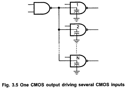
The CMOS output has to charge and discharge the parallel combination of all the input capacitances. This charging and discharging time increases as we increase number of loads. Typically, each CMOS load increases the driving circuit’s propagation delay by 3 ns. Thus, fan-out for CMOS depends on the permissible maximum propagation delay. Typically, CMOS outputs are limited to a fan-out of 50 for low-frequency operation (≤ 1 MHz). Of course, for high-frequency operation the fan-out would have to be less.
Power Dissipation (PD) : The power dissipation of a CMOS IC is very low as long as it is in a dc condition. Unfortunately, power dissipation of CMOS IC increases in proportion to the frequency at which the circuits are switching states. For example, a CMOS NAND gate that has PD =10 nW under DC conditions will have PD = 0.1 mW at a frequency of 100 kHz, and 1 mW at 1 MHz.
When CMOS output switches from LOW to HIGH, a transient charging current has to be supplied to the load capacitance. Therefore, as the switching frequency increases, the average current drawn from VDD also increases, resulting increase in power dissipation.
Propagation Delay : The propagation delay in the performance of CMOS Gates is the sum of delay due to internal capacitance and due to load capacitance. The delay due to internal capacitance is called the intrinsic propagation delay. The delay due to load capacitance can be approximated as follows :
tp(CL) ≈ 0.5 Ro CL seconds
- tP(CL) is either tpLH or tpHL
- Ro is the output resistance of the gate, and
- CL is the total load capacitance.
The Ro depends on the supply voltage and it can be approximated as
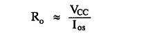
where Ios is the short circuit output current.
Unused Inputs : CMOS inputs should never be left disconnected. All CMOS inputs have to be tied either to a fixed voltage level (0V or VDD) or to another input. This rule applies even to the inputs of extra unused logic gates on a chip. An unused CMOS input is susceptible to noise and static charges that could easily bias both the P-and N-channel MOSFETs in the conductive state, resulting in increased power dissipation and possible overheating.
Static-charge Susceptibility (CMOS Hazards) : Every CMOS device is vulnerable to the building up of electrical charge on its insulated gate. Recall that the relationship between charge Q and voltage V on a capacitor having capacitance C is
V = Q/C
Since the input capacitance at the gate is usually quite small (a few picofarads), a relatively small amount of charge can create a large voltage which may be greater than the breakdown voltage of a MOS gate (typically 100 V).
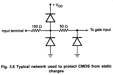
The primary source of charge is “static” electricity, usually produced by handling and the motion of various kinds of plastics and textiles. The CMOS devices are protected against this static charge by on-chip diode-resistor network, as shown in the Fig. 3.6. These diodes are designed to turn ON and limit the size of the input voltage to well below any damaging value.
Latch-up : CMOS integrated circuits contain parasitic PNP and NPN transistors : transistors that exist because of the proximity of P and N materials embedded in the substrate. Their existence is not intentional but is unavoidable. Because of conducting paths between a pair of such transistors, a device can be triggered into a heavy conduction mode, known as latch-up. This heavy conduction mode, results large current flow which can destroy IC. Most CMOS circuits contain protective measures to prevent latch-up, but it can still occur if the manufacturers specified maximum ratings are exceeded.