Combinational Circuit | Block Diagram | Design Procedure:
When logic gates are connected together to produce a specified output for certain specified combinations of input variables, with no storage involved, the resulting circuit is called Combinational Logic. In Combinational logic, the output variables are at all times dependent on the combination of input variables. A Combinational Circuit consists of input variables, logic gates, and output variables. The logic gates accept signals from the input variables and generate output signals. This process transforms binary information from the given input data to the required output data.
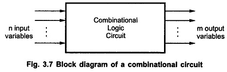
Block Diagram of Combinational Circuits:
Fig. 3.7 shows the block diagram of combinational circuits. As shown in Fig. 3.7, the combinational circuits accepts n-input binary variables and generates output variables depending on the logical combination of gates.
The design of combinational circuits starts from the outline of the problem statement and ends in a logic circuit diagram or a set of Boolean functions from which the logic diagram can be easily obtained.
Design Procedure:
The design procedure of the combinational circuits involves following steps,
- The problem definition.
- The determination of number of available input variables and required output variables.
- Assigning letter symbols to input and output variables.
- The derivation of truth table indicating the relationships between input and output variables.
- Obtain simplified Boolean expression for each output.
- Obtain the logic diagram.