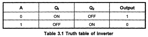
CMOS Inverter Working Principle:
CMOS Circuit contain both NMOS and PMOS devices to speed the switching of capacitive loads. It consumes low power and can be operated at high voltages, resulting in improved noise immunity. Fig. 3.1 shows the basic CMOS Inverter Working Principle.
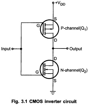
It consists of two MOSFETs in series in such a way that the P-channel device has its source connected to +VDD (a positive voltage) and the N-channel device has its source connected to ground. The gates of the two devices are connected together as the common input and the drains are connected together as the common output.
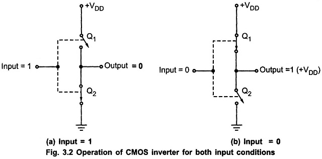
When input is HIGH, the gate of Q1 (P-channel) is at 0V relative to the source of Q1 i.e. VGS1 = 0V. Thus, Q1 is OFF. On the other hand, the gate of Q2 (N-channel) is at +VDD relative to its source i.e. VGS2 = +VDD. Thus, Q2 is ON. This will produce Vout ≈ 0 V, as shown in the Fig. 3.2 (a).
When input is LOW, the gate of Q1 (P-channel) is at a negative potential relative to its source while Q2 has VGS = 0 V. Thus, Q1 is ON and Q2 is OFF. This produces output voltage approximately +VDD, as shown in the Fig. 3.2 (b).
Table 3.1 summarizes the operation of CMOS Inverter Truth Table