Pin diagram of 8089 Processor:
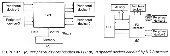
Pin diagram of 8089 Processor – In a microprocessor-based system, there are many peripheral devices which are interconnected with the main processor as shown in Fig. 9.102(a). To perform any operation related to peripheral devices, the CPU must initiate the specified operation and also track their operations. After completion of the input/output operation, CPU must be maintaining the post-operation status and records. Therefore, the CPU consumes some time for these operations and there will be always some delay in communication. To reduce the delay of operations related with peripheral devices, the I/O processor is used to control all input/output operations as depicted in Fig. 9.102(b). When operation is initiated by the main processor, the I/O processor receives a request from the system peripherals. I/O processors communicate with the main processor using its interrupt services.
The 8089 is an I/O processor in microprocessor input/output processing and is packaged in a 40-pin DIP package. The 8089 is a high-performance processor implemented in N-channel HMOS technology. The 8089s instruction sets are optimized for high speed, flexible and efficient I/O handling. It can work with 16-bit 8086 and 8-bit 8088 microprocessors with 8-bit and 16-bit peripherals. The communication with main processors is done using a memory table which states the details of the task to be executed. The memory table is prepared by the host processor to allot the specified task to the I/O processor. The host processor interrupts the I/O processor after sending a task to it. Then the I/O processor reads the memory table to get details of the allotted task. The memory table provides an address of the program written in the 8089 I/O processor instructions and it is called channel program. Then the 8089 I/O processor executes the channel program. Subsequently, the 8089 I/O processor can fetch and execute its own instructions. The features of 8089 I/O processors are as follows:
- High-speed DMA operations between I/O to memory, memory to I/O, memory to CPU, CPU to memory, and I/O to I/O
- Memory-based communication with CPU
- Can support local or remote I/O processing
- Compatible with 8086/8088 processors
- Flexible, intelligent DMA functions such as translation, search, and word
- Assembly/Disassembly
- Multi-bus compatible system interface
- 1 Mbyte addressability
- Interface with 8-bit and 16-bit peripherals
Figure 9.103 shows the pin diagram of 8089 and function of each Pin diagram of 8089 is explained below:
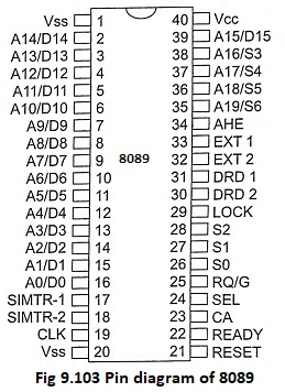
A15/D15-A0/D0(Input/Output) These lines are used as multiplexed address and data bus. A15-A8 are stable on transfers to a physical 8-bit data bus and are multiplexed with data on transfers to a 16-bit physical bus.
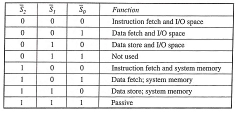
A19/S6-A16/S3(Output) These are multiplexed most significant address lines and status information as given below:
B̅H̅E̅ (Output) The Bus High Enable B̅H̅E̅ is used to enable data operations on the most significant half of the data bus D15-D8. when this signal is active low, a byte is to be transferred on the upper half of the data bus.
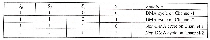
S̅2, S̅1, S̅0 (Output) These are the status pins which state the different activities of I/O processor as given below:
READY (Input/Output) This signal is received from the addressed device which indicates that the device is ready for data transfer.
L̅O̅C̅K̅ (Output) The lock output signal indicates to the bus controller that the bus requires more than one contiguous cycle.
RESET (Input) When the I/O processor receives the reset signal, the I/O processor has suspended its activities and enters an idle state until a channel attention is received.
The signal must be active for at least four clock cycles.
CLK (Input) Clock signal is required for internal I/O processor.
CA (Input) This is used as the channel attention signal of the I/O processor.
SEL (Input) The first CA received after reset informs the I/O processor through the SEL line, whether it is a master or slave and starts the initialization sequence.
DRQ2-DRQ1 (Input) These are the DMA request input signals of the I/O processor. These signals indicate that a peripheral is ready to transfer/receive data using either Channel-1 and Channel-2.
R̅Q̅/G̅T̅ (Input/Output) The request grant signal is used to implement the communication dialogue required to arbitrate the use of the system bus between IOP and CPU, LOCAL mode or I/O bus when two I/O processors share the same bus. The R̅Q̅/G̅T̅ is active low signal.
SINTR2-SINTR1 (Output) These are the interrupt output signals from Channel-1 and Channel-2 respectively.
EXT2-EXT1 (Input) These are external terminate input signals for Channel-1 and Channel-2 respectively. The EXT signal is used to terminate the current DMA transfer operation if the channel is so programmed by the channel control register.
Functional Description of 8089 Architecture
The 8089 I/O processor has been designed to remove I/O processing, control and high-speed transfers from the CPU. This processor can support I/O peripheral devices and also support versatile DMA data transfer. The DMA function can boast flexible termination conditions such as external terminate, mask compare, single transfer and byte count. The DMA function of the 8089 I/O processor uses a two-cycle approach where the information actually flows through the 8089 I/O processor. This method of DMA data transfer vastly simplifies the bus timings and enhances compatibility with memory and peripherals.
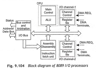
Figure 9.104 shows the block diagram of 8089 architecture. The 8089 I/O processor has two internal I/O channels. These two channels can be programmed independently to handle two separate I/O tasks for the host CPU. The ALU and main control unit are shared by both the channels. The main control unit generates the control signals for the operation of the I/O processor channels. The bus control unit handles all the bus activities. The Channel Control Pointer (CCP) is used by the programmers and gets loaded with the 20-bit address of a memory table for the channel. Actually, this table is prepared by the host CPU to allot a task to the I/O processor. The address of the memory table for Channel 2 is computed by adding 8 to the memory table address of channel 1 or the contents of CCP.
The communication between the CPU and I/O processor is performed through a look-up table in shared memory. The CPU sends a hardware Channel Attention (CA) signal to the I/O processor so that 8089 executes a program by placing it in the 8089’s memory space. The SEL pin in Pin diagram of 8089 indicates to the I/O processor about the select channel. The communication from the I/O processor to the host processor can be performed in a similar way through system interrupt signals SINTR2 and SINTR1 when the CPU enables interrupts. The 8089 is able to store messages in the memory regarding its status and the status of any peripherals. Usually, this communication mechanism is supported by a hierarchical data structure as depicted in Figure 9.105.
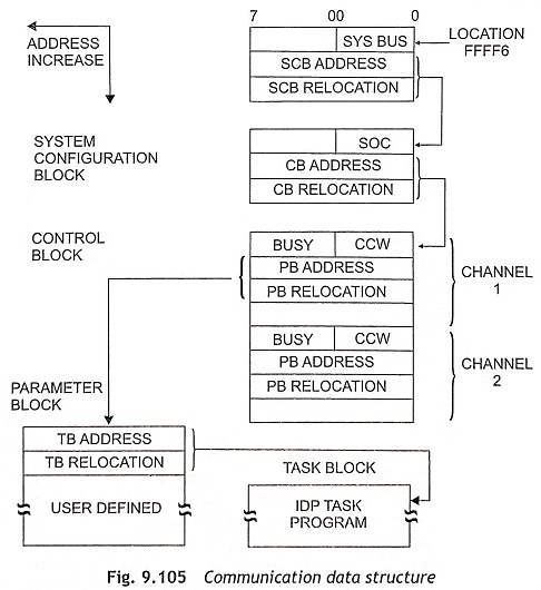
After the first CA from RESET, if the I/O processor is initialized as the BUS MASTER, 5 bytes of information are read into the 8089 starting at location FFFF6. Then information about the type of system bus and pointers to the system configuration block are obtained. This is the only fixed location to be accesses by the 8089. The remaining addresses are obtained through the data structure hierarchy.
The Pin diagram of 8089 computes addresses in the same way as 8086. The 20-bit address is generated by 4-bits left shifting of the 16-bit relocation pointer and added to the 16-bit address offset. Once 20-bit addresses are formed, they are stored in the 20-bit address registers of 8089. After the system configuration, pointer address is formed and the 8089 can access the System Configuration Block (SCB).
The SCB is used only during startup, points to the Control Block (CB) and provides I/O processor system configuration data via the SOC byte. The SOC byte initializes the I/O processor I/O bus width to 8 bits or 16 bits, and states one of two R̅Q̅/G̅T̅ operating modes. During R̅Q̅/G̅T̅ mode 0 operation, the I/O processor is initialized as SLAVE, and its R̅Q̅/G̅T̅ is line attached to a Master CPU. In this mode, the CPU has control of the bus, grants control to the IOP. For mode 1, the I/O processor is useful only in remote mode between two I/O processors (MASTER and SLAVE).
The control block performs the bus control initialization for the I/O processor operation and provides pointers to the parameter block or data memory for channels 1 and 2. The Channel Control Word (CCW) is retrieved and analyzed. The CCW byte is decoded to determine channel operation.
The parameter block contains the address of the task block and acts as a message center between the I/O processor and CPU. Parameters information is passed from the CPU to I/O processor in this block to adapt the software interface to the peripheral device. It is also used for transferring data and status information between the I/O processor and CPU.
The task block holds the instructions for the respective channel. This block can reside on the local bus of the I/O processor and the I/O processor can operate concurrently with the CPU. The advantage of the communication between the processor, I/O processor and peripherals is that it allows for a very clear method for the operating system to handle I/O routines.
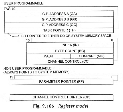
The 8089 has separate registers for its two different I/O channels as shown in Figure 9.106. Each channel has two sets of registers such as pointers and registers. The pointers are 20-bit registers usually used to address memory, but the registers are 16-bit general-purpose data registers. Each of the pointers excluding PP register has a tag bit. This bit is used to indicate that either the 20-bit register content is to be used or the lower 16-bit register content is to be used as the pointer.
The PP register is a 20-bit pointer. The registers GA, GB, GC, IX, BC and MC can be used as general-purpose registers, when they are not used as pointers. The memory operands can be accessed using one of the base pointers GA, GB, GC, and PP.
The basic DMA pointer registers (GA and GB) can point to the system bus or local bus, DMA source or destination, and can be automatically incremented. The register set GC can be used to allow translation during the DMA process through a look-up table. The channel control register can be accessed by MOV and MOVI instructions and the mode of the channel operation will be selected. Registers are also provided for a masked compare during the data transfer and can be set up to act as one of the termination conditions. Other registers can be used as general-purpose registers during program execution, while the I/O processor is not performing DMA cycles.
The 8089 I/O processor can be used in different applications such as file management in hard disk or floppy disk, soft error recovery routines and scan control, CRT control (cursor control and auto scrolling), keyboard control, communication control and general I/O applications.