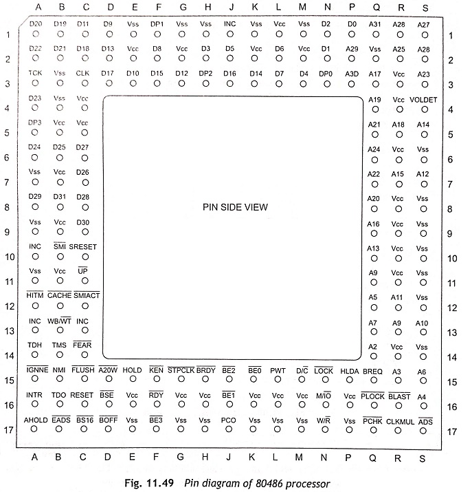
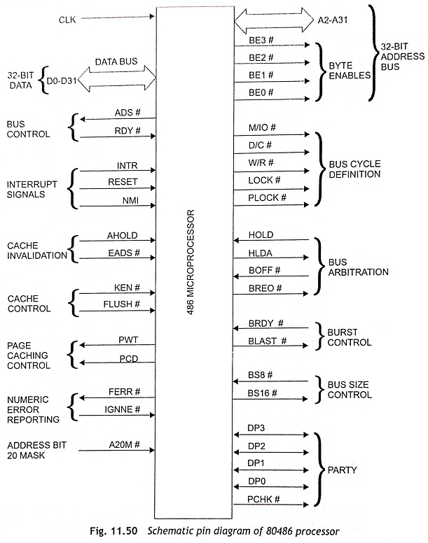
Pin Diagram of 80486 Microprocessor:
The pin diagram of 168-pin PGA (Pin Grid Array) package 80486 is shown in Fig. 11.49 and the schematic Pin Diagram of 80486 Microprocessor is depicted in Fig. 11.50. All signals of 80486 are grouped according to their functions. Some of the most important groups of signals are explained in this section.
CLK The CLK input signal provides the timing for the operation of 80486.
Address Bus
A31-A2 The address lines A31-A2 are used for selecting memory and I/O devices.
B̅E̅3-B̅E̅0 For memory and I/O addressing, byte enable signals B̅E̅3-B̅E̅0 are required. When the byte enable signals B̅E̅3-B̅E̅0 are active-low, these indicate which byte of the 32-bit data bus is active during the read or write cycle. For example, when B̅E̅0 = 0, the least significant byte is active. In the same way, if B̅E̅3 = 0, the most significant byte in 32-bit data is accessed.
Data Bus
D31-D0 The data lines D31-D0 are a bidirectional data bus. D31 is the most significant data bit and D0 is the least significant data bit.
Data Parity Group These pins are used to detect the parity during the memory read and write operations.
DP3-DP0 The four data parity input/output pins are DP3-DP0. These Pin Diagram of 80486 Microprocessor are used to represent the individual parity of 32 bits (4 bytes) of the data bus.
Bus Cycle Definition Group
M/I̅O̅ The M/I̅O̅ output pin is used to differentiate between memory and I/O operations.
W/R̅ The W/R̅ output pin is used to differentiate between read and write bus cycles.
D/C̅: This output pin can be used to differentiate between data and control Operations.
L̅O̅C̅K̅ This output pin is used to state that the current bus cycle is locked.
P̅L̅O̅C̅K̅ The P̅L̅O̅C̅K̅ (pseudo lock) output pin indicates that the current operation requires more than one bus cycle to complete the task. This signal is at logic level 0 for arithmetic co-processor operations.
Bus Control Group
A̅D̅S̅ The A̅D̅S̅ (address data strobe) output pin indicates that the address bus contains a valid memory address.
R̅D̅Y̅ The R̅D̅Y̅ (ready) input pin acts as a ready signal and this signal is used for the current non burst cycle.
Burst Control Group
B̅R̅D̅Y̅ The B̅R̅D̅Y̅ (burst ready) input pin indicates the burst mode of memory read or memory operation. During burst mode, the speed of memory access may be doubled compared to normal memory read/write operations.
B̅L̅A̅S̅T̅ When the B̅L̅A̅S̅T̅ (burst last) output signal is high, it indicates that CPU initiates the burst mode of memory access. If this signal is low, it indicates that the burst bus cycle is completed and the B̅R̅D̅Y̅ signal is next asserted for starting the next memory access operation.
Bus Arbitration Group
HOLD The HOLD pin acts as a local bus hold input. This pin may be activated by another bus master like DMA controller. This pin is functionally similar to the BREQ pin.
HLDA The HLDA output signal is used to acknowledge the receipt of a valid HOLD request.
BREQ When the BREQ (bus request) output signal is active-high, it indicates that the 80486 CPU has generated a internal bus request.
B̅O̅F̅F̅ When the B̅O̅F̅F̅ (back off) input pin is at logic level 1, 80486 CPU places its buses at hold state. The active-high back off input signal forces the current bus master of 80486 CPU to release the bus in the next clock cycle.
Interrupts
INTR The INTR pin is a maskable interrupt input. It is controlled by the IF in the flag register.
NMI This is a type-2 nonmaskable interrupt input.
RESET The RESET input pin is used to reset the processor when it becomes high.
Cache Control Group
K̅E̅N̅ The K̅E̅N̅ (cache enable) input pin is used to decide whether the current cycle is cacheable or not.
F̅L̅U̅S̅H̅ The F̅L̅U̅S̅H̅ is a cache flush input signal. When this pin is activated, it clears the cache contents and validity bits.
Cache Invalidation Group
AHOLD The AHOLD (address hold request) input signal enables other bus masters to use the 80486 system bus for a cache invalidation cycle.
E̅A̅D̅S̅ The E̅A̅D̅S̅ (external address) input signal is used to indicate that a valid address for external bus cycle is available on the address bus.
Page Cache Ability Group
PCD The PCD (page cache disable) output pin reflect the status of the PCD attribute bit in page table or page directory entry.
PWT The PWT (page write-through) output pin indicates the status of the PWT attribute bit in page table or page directory entry.
Bus Size Control Group
B̅S̅8̅ The B̅S̅8̅ (bus size 8) input pin is used for the 8-bit dynamic bus sizing feature of 80486 and the 80486 can be interfaced with 8-bit external devices.
B̅S̅1̅6̅ The B̅S̅1̅6̅ (bus size 16) input pin is used for the 16-bit dynamic bus sizing feature of 80486 and the 80486 can be interfaced with 16-bit external devices.
A̅2̅0̅M̅ When the A̅2̅0̅M̅ (address bit 20 mask) input pin is activated, the 80486 masks the physical address line A20 before performing any memory or cache cycle. This is very useful to wrap the physical address space from 00FFFFH to 000000H as the 8086 microprocessor does and it works around the 1 Mbyte memory size. i.e. physical memory space of 8086 in virtual 8086 mode.
FPU Error Group
FERR The FERR output signal is activated whenever the floating point unit generates any error.
IGNNE When the IGNNE (Ignore Numeric Processor Extension) input pin is activated, the 80486 ignores the floating processor (FPU) errors and execute non-control floating-point instructions continuously.
Test Access Port Group The test access is a unique facility, which is available in the 50 MHz version 80486. The test access signals are used to check the fault conditions of the components on the motherboard.
TDI The TDI (test data) input of 80486 is the serial input pin which is used to shift the JTAG instructions and data into components.
TCK The TCK (test clock) input provides the basic clock signal, which is required by the boundary test feature.
TDO The TDO (test data output) pin is the serial output pin which is used to shift the JTAG instruction and data out of components under test.
TMS The TMS (test mode select) input is decoded by the JTAG TAP (tap access port) to select the operation of this test logic.
Supply Lines
VCC The VCC pin is connected to +5 V power supply. There are 24 VCC pins in the 80486 processor. Ground Lines
VSS The VSS pin is connected to the ground terminal of power supply. There are 28 VSS pins in the 80486 processor.