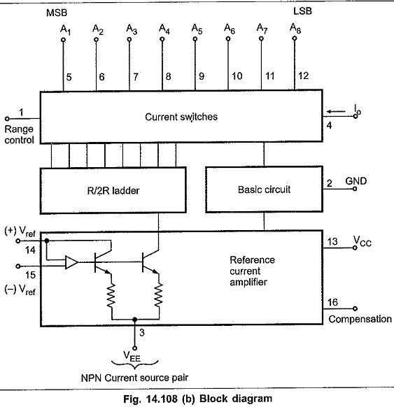
IC 1408 DAC Pin Diagram:
The IC 1408 DAC Pin Diagram is an 8 bit R/2R ladder type D/A converter compatible with TTL and CMOS logic. It is designed to use where the output current is linear product of an eight bit digital word. Fig. 14.108 shows the pin diagram and block diagram for IC 1408 DAC.
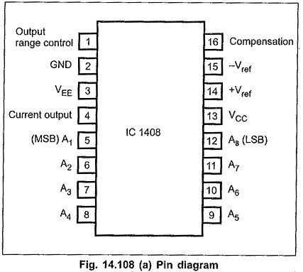
The IC 1408 DAC Pin Diagram consists of a reference current amplifier, an R/2R ladder and eight high speed current switches. It has eight input data lines A1 (MSB) through A8 (LSB) which control the positions of current switches.
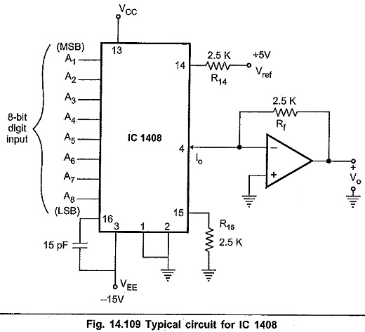
It requires 2 mA reference current for full scale input and two power supplies Vcc= + 5 V and VEE = – 15 V (VEE can range from – 5 V to – 15 V).
The voltage Vref and resistor R14 determines the total reference current source and R15 is generally equal to R14 to match the input impedance of the reference current amplifier.
Fig. 14.109 shows a typical circuit for IC 1408.
The output current Io can be given as

Note : Input A1 through A8 can be either 0 or 1. Therefore, for typical circuit full scale current can be given as,
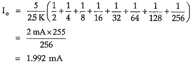
It shows that the full scale output current is always 1 LSB less than the reference current source of 2 mA. This output current is converted into voltage by I to V converter. The output voltage for full scale input can be given as

Note : The arrow on the pin 4 shows the output current direction. It is inward. This means that IC 1408 sinks current. At (0000 0000)2 binary input it sinks zero current and at (1111 1111)2 binary input it sinks 1.992 mA.
The circuit shown in the Fig. 14.109 gives output in the unipolar range. When digital input is 00H, the output voltage is 0V and when digital input is FFH (1111 1111)2, the output voltage is + 5 V. This circuit can be modified to give bipolar output.
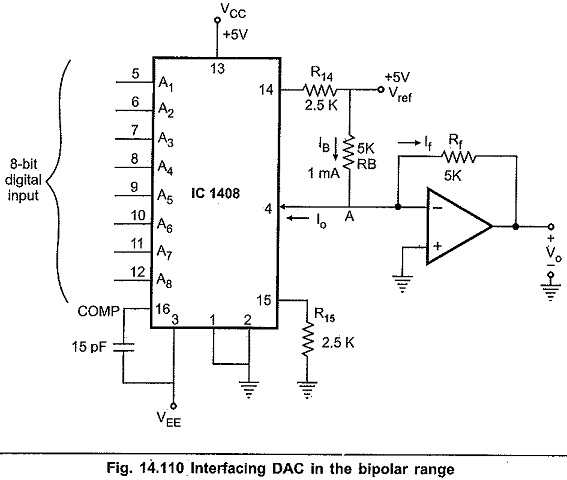
Fig. 14.110 shows the circuit for giving output in the bipolar range. Here, resistor RB (5 K) is connected between Vref and the output terminal of IC 1408 DAC Pin Diagram. This gives a constant current source of 1 mA.
The circuit operation can be observed for three conditions :
Condition 1 : For binary input (OOH)
When binary input is 00H, the output current Io at pin 4 is zero. Due to this current flowing through RB (1 mA) flows through Rf giving Vo = – 5 V.
Condition 2 : For binary input 80H
When binary input is 80H, the output current Io at pin 4 is 1 mA. By applying KCL at node A we get,
![]()
Substituting values of IB and Io we get,

and therefore the output voltage is zero.
Condition 3 : For binary input FFH
When binary input is FFH, the output current Io at pin 4 is 2 mA. By applying KCL at node A we get,
![]()
Substituting values of IB and Io we get,
![]()
Therefore, the output voltage is + 5V. In this way, circuit shown in the Fig. 10.15 gives output in the bipolar range.
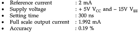
Important Electrical Characteristics for IC 1408: