ADC0808 Pin Diagram:
The ADC0808 Pin Diagram and ADC 0809 are monolithic CMOS devices with an 8-channel multiplexer. These devices are also designed to operate from common microprocessor control buses, with tri-state output latches driving the data bus.
The main features of ADC0808 Pin Diagram are :
- 8-bit successive approximation ADC.
- 8-channel multiplexer with address logic.
- Conversion time 100 μs.
- It eliminates the need for external zero and full-scale adjustments.
- Easy to interface to all microprocessors.
- It operates on single 5V power supply.
- Output meet TTL voltage level specifications.
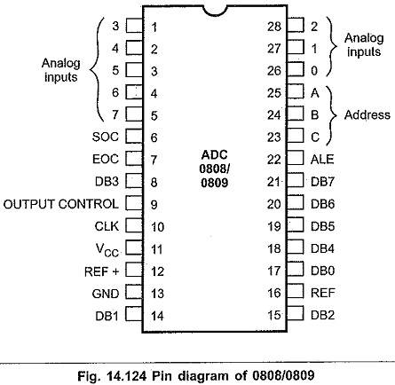
Pin Diagram of ADC0808 Pin Diagram:
Fig. 14.124 shows pin diagram of 0808/0809 ADC.
Operation of ADC0808 Pin Diagram:
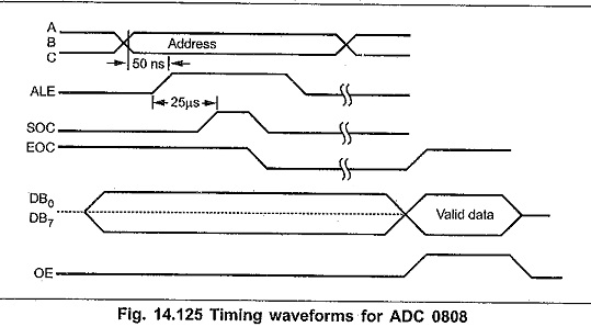
ADC 0808/0809 has eight input channels, so to select desired input channel, it is necessary to send 3-bit address on A, B and C inputs. The address of the desired channel is sent to the multiplexer address inputs through port pins. After at least 50 ns, this address must be latched: This can be achieved by sending ALE signal. After another 2.5 μs, the start of conversion (SOC) signal must be sent high and then low to start the conversion process. To indicate end of conversion ADC 0808/0809 activates EOC signal. The microprocessor system can read converted digital word through data bus by enabling the output enable signal after EOC is activated. This is illustrated in Fig. 14.125.
Interfacing of ADC0808 Pin Diagram:
Fig. 14.126 shows typical interfacing circuit for ADC 0808 with microprocessor system.
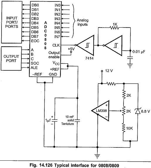
The zener diode and LM 308 amplifier circuitry is used to produce a VCC and +VREF of 5.12 V for the A/D converter. With this reference voltage the A/D converter will have 256 steps of 20 mV each.
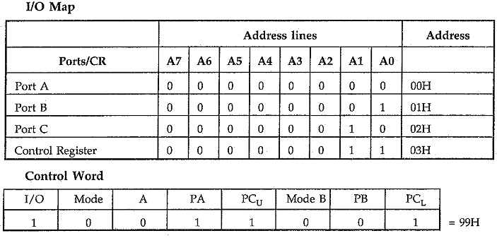
Interfacing ADC 0808 with 8085:
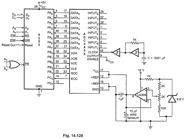
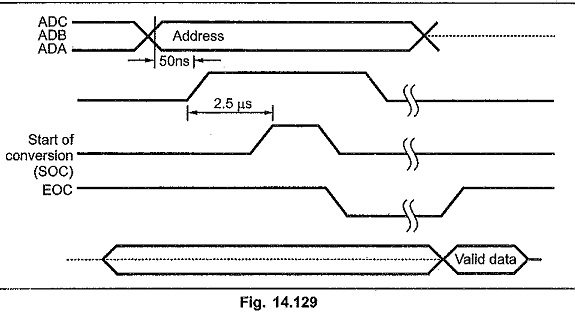
Fig. 14.128 shows interfacing of ADC 0808 with 8085 using 8255. ADC 0808 has eight input channels, so to select desired input channel, it is necessary to send 3-bit address on ADC, ADB and ADA inputs. The address of the desired channel is sent to the multiplexer address inputs through PB0 to PB2 lines.
After at least 50 ns, this address must be latched. This is achieved by sending ALE signal using Tort line PB3. After another 2.5 μs the start of conversion signal (SOC) must be sent high and then low. Port line PB4 is used for this purpose. The end of conversion (EOC) is detected by port line PC0. The Fig. 14.129 shows timing wave forms for the ADC 0808. Schmitt-trigger inverter circuitry generates 300 kHz clock which is required to operate ADC 0808. The zener diode and LM 308 amplifier circuitry is used to produce a VCC and +VREF of 5.12 V for the A/D converter. With this reference voltage the A/D converter will have 256 steps of 20 mV each.