80186 Pin Diagram:
The 80186 is a 68-pin IC and it is available in Plastic Leaded Chip Carrier (PLCC), ceramic Leadless Chip Carrier (LCC) and Pin Grid Array (PGA) packages. Figure 11.14 shows the 80186 Pin Diagram in ceramic leadless chip carrier package.
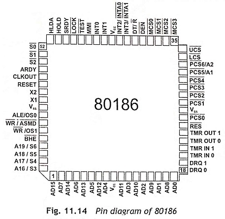
The pin functions are discussed elaborately as given below:
VCC (Input) +5 volt power supply
VSS (Input) Ground
RESET (Output) The output of RESET pin indicates that the 80186 CPU is being reset. It can also be used as a system reset. When it is logic level HIGH (1) and synchronized with the processor clock, it lasts an integer number of clock periods corresponding to the length of the R̅E̅S̅ signal.
X1, X2 (Input) The X1 and X2 are crystal input terminals. These 80186 Pin Diagram provide an external connection for a fundamental mode parallel resonant crystal for the internal crystal oscillator, but X1 can be used for interfacing an external clock instead of a crystal.
CLKOUT (Output) The clock output provides the system clock with a 50% duty-cycle waveform. Usually, the clock signal (CLKOUT) is generated when the input or oscillator frequency is internally divided by two, so that frequency of CLKOUT is one half of the crystal oscillator.
R̅E̅S̅ (I) When input is logic level LOW (0), the system will he reset. so that the 80186 immediately terminates its present operation, clears the internal logic, and enters into a dormant state. For proper reset operation, R̅E̅S̅ must be low for at least 50 ms. This signal may be asynchronous to the 80186 clock. Generally, this pin is connected to an RC circuit which generates a reset signal after application of power supply. When R̅E̅S̅ the 80186 will drive the status lines to an inactive level for one clock, and then tri-state them.
TEST (Input) The function of T̅E̅S̅T̅ input signal can be examined by the WAIT instruction. When the T̅E̅S̅T̅ input is HIGH, WAIT execution starts and instruction execution will be suspended. This input signal is synchronized internally.
TMR IN0, TMR IN1 (Input) These are timer input signals which are used either as clock or control signals, depending upon the programmed timer mode. Usually, these inputs are active HIGH or logic level 1 and internally synchronized.
TMR OUT 0, TMR OUT 1 (Output) These are timer output signals which are used to provide a single pulse or a continuous waveform generation, depending upon the selected timer mode.
DRQ0, DRQ1 (Input) The DRQ0 and DRQ1 are DMA request inputs for two internal DMA channels. These pins are driven HIGH by an external device whenever it is required to perform data transfer though DMA channel 0 or 1. These signals are active HIGH, level-triggered, and internally synchronized.
NMI (Input) NMI (Non-Maskable Interrupt) is an positive edge-triggered input which causes a type 2 It is not maskable internally. This signal is latched internally and is also internally synchronized. NMI duration of one clock or more will guarantee service.
INT0, INT1(Input) INT2/INTA0(I/O), INT3/INTA1(I/O) The maskable interrupt requests can be requested by one of INT0, INT1, INT2/INTA0 and INT3/INTA1 pins. Usually, these input pins are active HIGH and are synchronized internally. INT2 and INT3 can be configured through software to provide active-LOW interrupt-acknowledge output signals. All interrupt inputs can be configured through software to be either edge-triggered or level-triggered. To ensure the interrupt operation, all interrupt requests must remain active until the interrupt is acknowledged.
A19/S6, A18/S5, AI7/S4, AI6/S3 (Output) A19-A16 are address bus outputs and S6-S3 are bus cycle statuses. These signals are used as the four most significant address bits during T1. Generally, these signals are active HIGH. During T2, T3, TW, and T4, status information is available on these lines, S6 differentiates processor cycle and DMA cycle. S6 = 0 indicates processor cycle and S6 = 1 indicates DMA cycle. S3,S4, and S5 are defined as LOW during T2-T4.
AD15-AD0 (I/O) These signals are time multiplexed address/data bus. During T1, the 80186 places A 15 to A0 signals on these pins to locate the memory or I/O address. During T2, T3, TW, and T4, these lines work as data bus. The bus is always active HIGH.
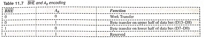
B̅H̅E̅/S7 (Output) The bus high enable signal can he used to determine if data is to be enabled onto the most significant half of the data bus, pins D15-D8 during T1 clock cycle. For any read, write, an interrupt acknowledge operations B̅H̅E̅ is LOW during T1 and a byte is to be transferred on the higher half of the bus. The S7 status is available during T2, T3 and T4 clock cycle. S7 is always at logic level 1. Hence no latch is required to de-multiplex S7. The function of processor depends on B̅H̅E̅ and A0 its shown in Table 11.7.
ALE/QS0 (Output) The ALE/QS0 (Address Latch Enable/Queue Status 0) is provided by the 80186 Pin Diagram to latch the address into the 8282 / 8283 address latches. When ALE is active HIGH, addresses are valid on the trailing edge of ALE.
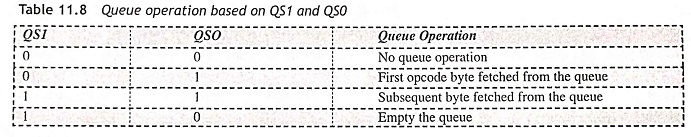
W̅R̅/QSI (Output) The W̅R̅/QSI (Write Strobe/Queue Status 1 ) is used to indicate that the data on the bus is to he written into a memory or an I/O device. The W̅R̅ signal is active for T2, T3 and TW of any write When the 80186 is in queue status mode, the ALE/QSO and W̅R̅/QSI pins give information about processor and instruction queue interaction as depicted in Table 11.8.
R̅D̅/Q̅S̅M̅D̅ (O) This signal is used indicate that the 80186 is performing a memory or I/O read cycle. The R̅D̅ is active LOW during T2, T3 and TW of any read cycle. R̅D̅ is driven HIGH for one clock during reset, and then the output driver is floated. During RESET, the pin is sampled to determine whether the 80186 should provide ALE, W̅R̅ , and R̅D̅, or the queue-status should be provided. R̅D̅ must be connected to GND (ground) to provide queue-status data.
ARDY(Input) The asynchronous ready input signal is used to inform the 80186 processor that the addressed memory or I/O device will complete a data transfer. This signal is internally synchronized by the 80186 on rising edge of the clock. The ARDY input pin will accept an asynchronous input, and is active When this pin is connected to +Vcc (+5 V), the 80186 functions normally. If this pin is connected to around. the 80186 enters WAIT states.
SRDY (Input) The synchronous ready input signal should be synchronized externally to the 80186. This signal can be used as the ready input. This line is active When this line is connected to Vcc, no WAIT states are inserted. The ARDY (Asynchronous Ready) or SRDY (synchronous ready) must be active before a bus cycle is terminated. When SRDY line is unused, it may remain connected to +5 V or it may be connected to ground.
L̅O̅C̅K̅ (Output) The L̅O̅C̅K̅ output signal is used to prevent other bus masters from accessing the system Usually, the LOCK signal is requested by the L̅O̅C̅K̅ prefix instruction while L̅O̅C̅K̅ is active LOW for the duration of locked instruction. This is activated at the beginning of the first data cycle connected with the instruction following the L̅O̅C̅K̅ prefix. It will be active until the completion of the instruction following the L̅O̅C̅K̅ prefix.
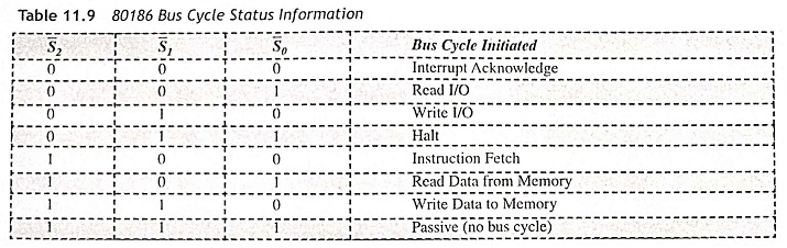
S̅2̅, S̅1̅, S̅0̅ (Output) The bus cycle status output signals S2-S0 are used to provide bus-transaction information as given in Table 11.9.
S̅2̅ can he used for a logical M/I̅O̅ signal, and S̅I̅ is used for DT/R̅ indicator. These status lines are active
HIGH for one clock during reset, and then floated until a bus cycle begins.
HOLD (Input) The HOLD signal is used to indicate whether any other bus master is requesting the local This input is active HIGH and it may be asynchronous with respect to the 80186 Pin Diagram clock.
HLDA (Output) After receiving a HOLD request, the 80186 will issue an HLDA hold acknowledge signal at the end of T4 or T1. Then the 80186 will float the local bus and control lines.
U̅C̅S̅ (Output) The U̅C̅S̅ (Upper Memory Chip Select) output signal is an active LOW whenever a memory reference is made to select the upper portion of the memory map. This output line is software programmable to enable memory size of 1KB -256KB.
L̅C̅S̅ (Output) The L̅C̅S̅ (Lower Memory Chip Select) is active LOW whenever a memory reference is made to select the lower portion of the memory map. This output line is also software programmable to enable memory size of 1 KB-256 KB.
MCS0-3 (Output) The midrange memory chip select signals, M̅C̅S̅0-3 are active LOW when a memory reference is made to the specified midrange portion of memory (8K-512K). These lines are not floated during bus HOLD and are software programmable.
P̅C̅S̅0-4 (Output) The peripheral chip select signals P̅C̅S̅0-4 are active LOW when a reference is made to the specified peripheral area about 65k byte I/O space. These lines are not floated during bus HOLD, but the address ranges are software programmable.
P̅C̅S̅5̅/Al(Output) The peripheral chip select 5 or latched address signal A1 can be programmed to provide a sixth peripheral chip select, or to supply an internally latched A1 signal. The address range activated by PCS5 is software programmable.
P̅C̅S̅6̅/A2(Output) The peripheral chip select 6 or latched address signal A2 may be programmed to provide a seventh peripheral chip select, or to give an internally latched A2 signal. The address range activated by PCS6 is also software programmable.
DT/R̅ (Output) The DT/R̅ (Data Transmit/Receive) signal controls the direction of data flow through the external data bus transceiver. If DT/R̅ is LOW, data is transferred to the 80186. When DT/R̅ is HIGH, the 80186 writes data on the data bus.
D̅E̅N̅ (Output) The D̅E̅N̅ (Data Enable) is used enable the external data bus transceiver output. This is active LOW during each memory and I/O access. If D̅E̅N̅ is HIGH, DT/R̅ changes state.