80186 Microprocessor Architecture:
The Intel 80186 Microprocessor is a high-performance, highly integrated 16-bit microprocessors. Usually, the 80186 Microprocessor is intended for embedded systems, as microcontrollers with external memory. To reduce the number of chips in systems, it is required to include clock generator, interrupt controller, timers, wait state generator, DMA channels, and external chip select lines within a chip. The 80186 is a natural successor to the 8086 in personal computers. However, because of its integrated hardware was incompatible with the hardware used in the original IBM PC. The architecture of 80186 Microprocessor is shown in Fig. 11.1.
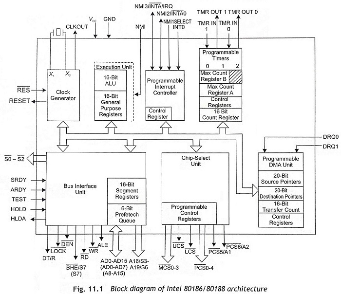
Th architecture of 80186 is common with the 8086 and 8088 microprocessors. This 80186 Microprocessor is a very high-integration 16-bit microprocessor. This IC combines 15 to 20 most common microprocessor components onto a single chip and provides twice the performance of standard 8086. The object code of 80186 is compatible with 8086 and 8088 microprocessors but it adds 10 new instructions. The following functional description describes the basic architecture of 80186 Microprocessor:
- Clock generator
- Bus interface unit
- DMA controller
- 16-bit programmable timer consisting of three timers
- Programmable interrupt controller
- Chip select unit into a single chip
The 8086, 8088, 80186, and 80286 families all contain the same basic set of registers, instructions, and addressing modes. The 80186 Microprocessor is also compatible with the 8086, 8088, and 80286 CPUs.
Register Set:
The 80186 base architecture has fourteen registers as shown in Fig. 11.2. These registers are grouped into the five categories such as segment registers. base and index registers, status and control registers and status word.
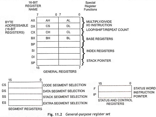
General Registers The 80186 Microprocessor consists of eight 6-bit general-purpose registers which are used to perform all arithmetic and logical operations. Four of these registers AX, BX, CX, and DX can be used as 16-bit registers or split into pairs of separate 8-hit registers.
Segment Registers Four 16-bit special-purpose registers (CS, DS, SS and ES) are used to select the segments of memory at any given time. The memory can be immediately addressable as code, stack, and data.
Base and Index Registers Four of the general-purpose registers BX, BR SI and DI can be used to determine offset addresses of operands in memory. These registers may contain base addresses or indexes to particular locations within a segment. The different addressing modes of the 80186 Microprocessor selects the specific registers to determine the physical address of memory for an operand.
Status and Control Registers Two 16-bit special-purposes registers (IP and Status word) are also used to record or alter different aspects of the 80186 Microprocessor state. The IP (Instruction Pointer) register contains the offset address of the next sequential instruction to be executed, but the status word register contains status and control flag bits as depicted in Fig. 11.2 and Fig. 11.3 respectively.
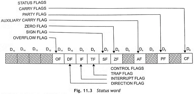
Status Word:
The status word is used to record specific characteristics of the result of logical and arithmetic instructions and controls the operation of the 80186 within a specified operating mode. The status word register is 16 bits wide. Bits 0, 2, 4, 6, 7, and 11 are used for logical and arithmetic operations and bits 8, 9, and 10 are used to control the processor operation. The function of the status word bits is given below.
CF (Carry Flag) The carry flag is set whenever a carry/barrow is generated after arithmetic operations such as addition and subtraction; cleared otherwise.
PF (Parity Flag) This flag is set if low-order 8 bits or the final result after arithmetic/logical operations contain an even number of 1 bit. If there is odd number of ones, it is reset.
AF (Auxiliary Flag) This AF is set whenever there occurs a carry or borrow at the low-order four bits of AL during any operations; cleared otherwise.
ZF (Zero Flag) This flag is set if the result is zero after any operation; otherwise it is reset.
SF (Sign Flag) The sign flag is equal to high-order bit of result. It is set if the result is negative or MSB = 1. It is reset if the result is positive or MSB = 0.
TF (Single-Step Flag) It is used in the processor in single-step mode. When this flag is set, a single-step interrupt occurs after the next instruction executes. TF is cleared by the single-step interrupt.
IF (Interrupt-Enable Flag) When this flag is set, maskable interrupts is enabled cause the CPU to control to an interrupt vector specified location.
DF (Direction Flag) If DF is set, it causes string instructions to auto-decrement the appropriate index register. Clearing DF causes auto-increment. When DF = 1, index register automatically decrement. If DF = 0, index register automatically increment.
OF (Overflow Flag) When the signed result is too large and cannot be expressed within the number of bits in the destination operand, overflow flag is set; cleared otherwise.
Clock Generator:
The 80186 has an on-chip clock generator for both internal and external clock generation. The features of the clock generator are a crystal oscillator, a divide-by-two counter, synchronous and asynchronous ready inputs, and reset circuitry.
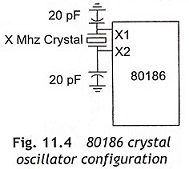
Oscillator Figure 11.4 shows the 80186 crystal oscillator configurations. The oscillator circuit of the 80186 is designed to be used with a parallel resonant fundamental mode crystal. This can be used as the time base for the 80186. The crystal frequency selected will be double the CPU clock frequency. When an external oscillator is used, it can be connected directly to the input pin X1 in lieu of a crystal. The output of the oscillator is not directly available outside the 80186 Microprocessor.
Clock Generator The 80186 clock generator provides the 50% duty cycle processor clock for the 80186. It is possible by dividing the oscillator output by 2 forming the symmetrical clock. When an external oscillator is used, the state of the clock generator will change on the falling edge of the oscillator signal. If an external crystal of 12 or 16 MHz is connected with 80186, then it generates a 6 or 8 MHz internal clock. Hence 80186/80188 is able to operate either at 6 or 8 MHz internal clock. The requirement of crystal frequencies for 80186/80188 is 16 MHz and for advanced version, the 80186/80188 is 12 MHz. The CLKOUT pin gives the processor clock signal for use outside the 80186. This can be used to drive other system components. Always all timings should be referenced to the output clock.
DMA Channels:
The 80186 DMA controllers have two independent high speed DMA channels. Data transfers can take place between memory and I/O devices (memory to I/O or I/O to memory) or within the same space (memory to memory or I/O to I/O). Data can be transferred either in 8 bits (bytes) or in 16 bits (words) from even or odd addresses. Each DMA channel consists of a 20-bit source and destination pointer. The content of the index pointer can be incremented or decremented depending upon data-transfer byte or word. When data transfer is one byte, the pointer is incremented by one. If data transfer is one word, the pointer is incremented by two. Each data transfer always takes 2 bus cycles, i.e., minimum 8 T states. The first bus cycle is used to fetch data and the other bus cycle can be used to store data. The maximum data transfer rate is about one Mword/s or 2 MBytes/s. Figure 11.5 shows the DMA block diagram of 80186.
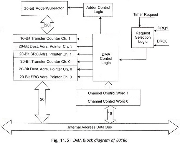
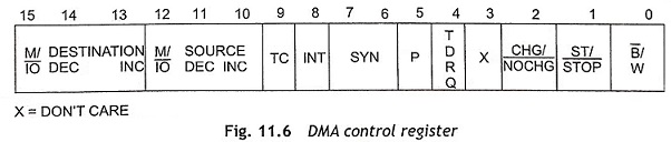
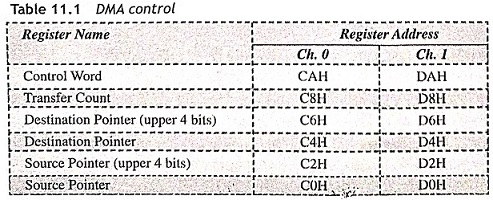
DMA Operation Each DMA channel consists of six registers in the control block which defines each channel’s specific operation. The control register has a 20-bit source pointer, a 20-bit destination pointer, a 16-bit transfer counter, and a 16-bit control word. The source pointer and destination pointer have two-words capacity as shown in Table 11.1 The number of DMA transfers to be performed is specified by the Transfer Count Register (TC). A maximum of 64 K byte or word transfers can be performed with automatic termination. The control word defines the channel’s operation. The content of all registers may be changed or modified during any DMA operation. Any changes in the registers must be reflected immediately in DMA operation. The DMA control register is depicted in Fig. 11.6.
DMA Channel Control Word Register Each DMA channel control word specifies the mode of operation for any particular 80186 DMA channel. The control word registers states
- The mode of synchronization
- The number of bytes or words to be transferred
- Interrupts to be generated after the last DMA data transfer
- Ceasing of DMA operation after a programmed number of DMA cycles
- The relative priority of one DMA channel with respect to the other DMA channel
- Whether the source pointer will be incremented, decremented, or maintained constant after each DMA operation
- Whether the source pointer addresses memory or I/O devices
- Whether the destination pointer will be incremented, decremented, or maintained constant after each DMA operation
- ‘Whether the destination pointer will address memory or I/O devices
Usually, the DMA channel control registers can be changed at the same time when the channel is operating. But any changes in the DMA channel control registers made during operation will affect the current DMA transfer.
DMA Control Word Bit Descriptions
B̅ / W: Byte/Word Transfers. If B̅/W = 0, a byte will be transferred. When B̅/W = 1, a word will be transferred.
ST/S̅T̅O̅P̅: Start/stop Channel. When ST/S̅T̅O̅P̅ = 1, the specified channel starts data transfer. While ST/S̅T̅O̅P̅ = 0, the specified channel should stop data transfer.
CHG/N̅O̅C̅H̅G̅: Change/Do not change ST/STOP bit. When CHG/N̅O̅C̅H̅G̅ bit is set during writing to the control word, the ST/S̅T̅O̅P̅ bit will be programmed by the write to the control word. If CHG/N̅O̅C̅H̅G̅ bit is cleared when writing the control word, the ST/S̅T̅O̅P̅ bit will not be changed. This bit cannot be stored and will always will be 0 on read.
INT This bit is used as enable interrupts to CPU on byte count termination.
TC While TC is set, DMA operation will be terminated if the contents of the transfer count register becomes zero. The ST/S̅T̅O̅P̅ bit will be reset, if TC is set. If TC bit is cleared, the content of transfer count register in the DMA unit will be decrement for each DMA cycle operation. Although the DMA transfer will not stop when the content of the TC register becomes zero.
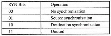
SYN: Synchronization bits (2 bits) The operation of synchronization bits is given below:
SOURCE INC Depending B̅/W, on increment source pointer by 1 or 2 after each transfer. If B̅/W = 0, increment source pointer by 1. When B̅/W = 1, increment source pointer by 2.
M/I̅O̅ The source pointer is in M/I̅O̅ space. If M/I̅O̅ is set ( 1 ), the source pointer represents memory. When M/I̅O̅ = 0, the source pointer represents input/output device address.
DEC Depending B̅/W, decrement the source pointer by 1 or 2 after each transfer. If B̅/W = 0, decrement the source pointer by 1. When B̅/W = 1 , decrement the source pointer by 2.
DEST: INC Increment the destination pointer by 1 or 2 after each transfer. When B̅/W = 0, increment the destination pointer by 1. If B/W̅ = 1, increment the destination pointer by 2.
M/I̅O̅ Destination pointer is in M/I̅O̅ space. When M/I̅O̅ is set (1), the destination pointer represents If M/I̅O̅ = 0, the destination pointer represents an input/output device address.
DEC Depending on B̅/W, decrement the destination pointer by 1 or 2 after each DMA data transfer.
P This bit stands for channel priority relative to other channel. Logic level 0 represents low priority and logic level 1 represents high priority. If channels are set at the same priority level, the operation of channels will alternate cycles.
TDRQ If this bit is reset (0), disable DMA requests from the timer 2. When it is set (1) , enable DMA requests from timer 2.
Bit 3 Bit 3 of DMA control register is not used.
Timers:
The 80186 microprocessor has three internal 16-bit programmable timers as depicted in Fig. 11.7. Two of these timers are highly flexible and programmable to count the external events and they are connected to four external pins (2 per timer). These two timers can be used to count external events, time external events, and generate non-repetitive waveforms. The third timer is not connected to any external pins. This timer can be used to interrupt the 80186 after a programmed interval of time to provide a count pulse to DMA unit, real-time coding and time delay applications.
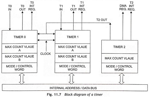
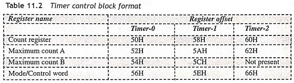
Timer Operation Usually, timers arc controlled by 11 16-bit registers in the internal peripheral control block. The timer control block format is demonstrated in Table 11.2. The count register contains the current value of the tinier and the timer count value can be read or written at any time when the timer is running or not running. The value of this register can be incremented after each timer event, Each of the timers is incorporated with a MAX COUNT register. In general, the MAX COUNT register is used to express the maximum count value of the timer. After reaching the MAX COUNT register value, the timer count value will reset to zero: so that the maximum count value is never stored in the count register itself. A second MAX COUNT register is also present in the timers 0 and 1 . This second MAX COUNT register enables the timers 0 and 1 to swap their count between two different MAX COUNT values which is programmed by the programmer.
As each timer gets a signal on every fourth CPU clock cycle, it can operate at speeds of up to one-quarter the internal clock frequency. External clocking of the timers can be done at the rate of one-quarter of the internal CPU clock rate. When the internal clock frequency is about 8 MHz, the timer operating frequency is 2 MHz. Any timer output can take maximum six clocks to respond to any individual clock or gate input due to internal synchronization and pipelining of the timer circuitry. As the count registers and the maximum count registers are 16 bits wide, 16 bits of resolution are provided in timers. For any read or write operation, the timers will add one wait state to the minimum four-clock bus cycle. This operation is required for synchronization and coordination between the internal timers and the internal bus for the internal data flows. The timers can be programmed in different modes as given below:
- Timer 0, Timer 1 and Timer 2 can be set to halt or continue on a terminal count.
- Timer 0 and Timer 1 can select between internal and external clocks, exchange between MAX COUNT registers and be set to retrigger on external events.
- The timers may be programmed to detect an interrupt on terminal count.
All the above modes of timer operation are selectable through the timer mode/control ward register.
Timer Mode/Control Register Usually, the mode/control register is used to allow the user to program in the specific mode of operation. It is also used to check the current programmed status for any of the three timers. Figure 11.8 shows the timer mode/control register. The operation of tinier mode/control register bits are discussed in this section.
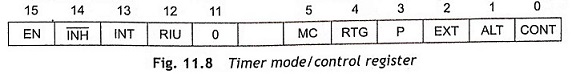
ALT The ALT bit is used to find out which of two MAX COUNT registers is used for count comparison. If ALT is logic level zero, Register A for that timer is always used, while if ALT is logic level one, the comparison will alternate between Register A and Register B when each maximum count is reached. This ALT bit can also be used to determine the function of the timer output pin. If ALT is logic level zero, the output pin will go LOW for one clock, the clock after the maximum count is reached, If ALT is logic level one, the output pin will reflect the current MAX COUNT register being used. Logic level 0 is used for Register B and logic level 1 is used for Register A.
CONT (Count) When the CONT bit is set, the associated timer runs continuously. If the CONT bit is reset, the timer will halt upon maximum count. While CONT = 0 and ALT = 1 , the timer will count to the MAX COUNT Register A value.
EXT (External Bit Selects) This bit selects between internal and external clocking for the timer. When this bit is set, the timer will count low-to-high transitions on the input pin. If it is cleared, it will count an internal clock while using the input pin for control. This external bit signal may be asynchronous with respect to the 80186 clock.
P (Prescaler) The prescaler bit must be ignored when internal clocking is not selected (EXT-0). When the P bit is at logic level zero, the timer will count at one-fourth the internal clock frequency. If the P bit is at logic level one, the output of Timer 2 can be used as a clock for the timer.
RTG (Retrigger) The RTG (Retrigger) bit is only active for internal clocking when EXT = 0. When RTG = 0. the input level gates the internal clock on and off. If the input pin is HIGH, the timer will count otherwise the timer will hold its value. If RTG = 1, the input pin is used to detect the low-to-high transitions. The first such transition starts the timer running, clearing the timer value to zero on the first clock, and subsequently increase. The next transitions on the input pin will again reset the timer to zero, from which it will start counting up again. The input signal may be asynchronous with respect to the 80186 clock.
EN (Enable) The EN (enable) bit gives the programmer control over the timer’s RUN/HALT status. If this bit is set, the timer is always enabled to increment depending upon the input pin constraints in the internal clock mode. When this bit is reset, the timer will be inhibited from counting.
INH (Inhibit) The INH (inhibit) bit is used to allow for selective updating of the EN (enable) bit. If INH is a logic level one while writing to the mode/control word, the state of the EN bit will be modified by the write operation. When INH is a logic level zero during the write, the EN bit will not be affected by the This bit will always be a 0 on a read operation.
INT (Interrupts) When this bit is set, the INT bit enables interrupts from the timer, which will be generated on every terminal count. If this enable bit is reset after the interrupt request has been generated, but before a pending interrupt is serviced, the interrupt request is latched in the Interrupt Controller.
MC (Maximum Count) The MC (Maximum Count) bit is set when the timer reaches its final maximum count value. This bit is set regardless of the timer’s interrupt-enable bit. The MC bit provides information to the programmer about the ability to monitor timer status through software instead of through interrupts.
RIU (Register In Use) The RIU (Register In Use) bit is used to indicate which MAX COUNT register is currently being used for comparison to the timer count value. When RIU = 0, it indicates Register A. The RIU bit cannot be written and its value is not changed when the control register is written. This bit is always cleared when the ALT bit is zero.
Count Registers Each timer has a 16-bit count register. The contents of this register can be read or written by the processor at any time. If we write in the register while the timer is counting, the new value will take effect in the current count cycle.
Max Count Registers Timer 0 and Timer 1 have two MAX COUNT registers, but Timer 2 has a single MAX COUNT register. The MAX COUNT registers are used to store the number of events that the timer will count. In Timer 0 and Timer 1. the MAX COUNT register can exchange between the two maximum count values whenever the current maximum count is reached.
Interrupt Controller:
The 80186 can receive interrupts from both internal and external sources. The internal interrupt controller is able to merge all interrupt requests on a priority basis and provides individual interrupt service by the CPU. Timers and DMA channels are the internal interrupt sources and these sources can be disabled by their own control registers. These can also be disabled by mask bits within the interrupt controller. The 80186 interrupt controller has control registers which can set the mode of operation for the controller.
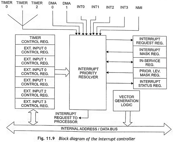
The interrupt controller can always resolve priority among all pending requests simultaneously. So interrupt service routines for lower priority interrupts might be interrupted by higher priority interrupts. The block diagram of the interrupt controller is shown in Fig. 11.9.
The interrupt controller is able to operate in two different modes such as
- non-iR MX 86 (Master) mode, and
- non-iR MX 86 (Master-Slave) mode.
Non-iRMX (Master) Mode Operation The interrupt controller provides five dedicated pins for external interrupt sources. One of these pins is Nonmaskable Interrupt (NMI). This pin is used for power-fail interrupts, etc. The other four pins may function either as four interrupt input lines with internally generated interrupt vectors, as an interrupt line and an interrupt acknowledge line along with two other input lines with internally generated interrupt vectors. While the interrupt lines are used in cascade mode, the 80186 interrupt controller will not generate internal interrupt vectors. In the cascade mode, external sources use externally generated interrupt vectors. If an interrupt is acknowledged, two INTA cycles are initiated and the vector is used to read into the 80186 on the second cycle. In cascade mode, external 8259A programmable interrupt controllers can be interfaced with the 80186 Microprocessor.
The basic modes of operation of the interrupt controller in non-iRMX mode (Master) are like the 8259A. The interrupt controller responds identically to internal interrupts in all three modes, namely, fully nested mode, cascade mode and special fully nested mode. But the difference of three modes is only in the interpretation of function of the four external interrupt pins. The interrupt controller can be set into one of the three modes after programming the INT0 and INT1 control registers.
Fully Nested Mode In the fully nested mode, four pins are used as direct interrupt requests. The vectors for these four inputs are generated internally. An in-service bit is provided for every interrupt source. If a lower-priority device requests an interrupt while the in-service bit (IS) is set, no interrupt will be generated by the interrupt controller. While interrupts are received and enabled, higher-priority interrupts will be serviced. When a service routine is completed, the proper IS bit must be reset by writing the proper pattern to the EOI register. An EOI command is issued at the end of the service routine just before the issuance of the return from interrupt instruction.
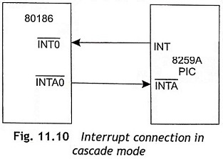
Cascade Mode In cascade mode, the 80186 has four interrupt pins and two of them have dual functions. In the fully nested mode, the four pins are used as direct interrupt inputs and the corresponding vectors are generated internally. In the cascade mode, the four pins are configured into interrupt input-dedicated acknowledge signal pairs. The interconnection between 80186 and 8259A is shown in Fig. 11.10. INT0 is an interrupt input which is used to interface an 8259A and INT2/INTA0 provides the dedicated interrupt acknowledge signal. The same is true for INT1 and INT3/INTA1 . The primary cascade mode allows the capability to serve up to 128 external interrupt sources through the use of external master and slave 8259As. Three levels of priority are created, requiring priority resolution in the 80186 interrupt controller, the 8259A masters, and the 8259A slaves.
Special Fully Nested Mode The interrupt controller operates in this mode after setting the SFNM bit in INT0 or INT1 control register. This mode enables complete nest ability with the external 8259A masters. Usually, any interrupt request from an interrupt source will not be recognized until the in-service bit for that source is reset.
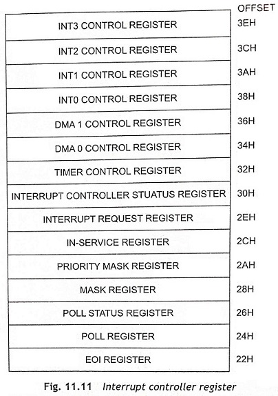
Interrupt Controller Registers The interrupt controller register is depicted in Fig. 11.11. It consists of fifteen registers such as in-service register, interrupt request register, mask register, priority mask register, interrupt status register, timer control register, DMA 0, 1 control registers, INT0-INT3 control registers, poll register, poll status register and EOI register. All registers can both be read or written to unless specified.
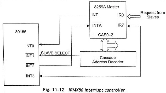
iRMX 86 Mode The interrupt controller has a special iRMX 86 compatibility mode that allows the use of the 80186 within the iRMX 86 operating system interrupt structure. This interrupt model requires one master and multiple slaves 8259A in cascade connection. In the iRMX mode, the internal 80186 interrupt controller will he used as a slave controller to an external master interrupt controller. Figure 11.12 shows the iRMX 86 interrupt controller interconnection. The INT0 input is used as the 80186 CPU interrupt input. INT3 functions as an output to send the 80186 slave-interrupt request to one of the eight master PIC inputs. To get correct master-slave interfacing, decoding of slave address CAS0-CAS2 are required. INT1 is used as slave-select input. INT2 is used as an acknowledge output and it is used to drive the INTA input of an 8259A.
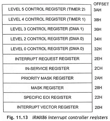
The iRMX mode of operation allows nesting of interrupt requests. Vector generation in the iRMX mode is exactly like that of an 8259A slave. In iRMX mode, the specific EOI command operates to reset an in-service bit of a specific priority. All control and command registers such as interrupt vector register, specific EOI register, mask register, priority-level mask register, in-service register, interrupt request register, and Level 0-Level 5 control registers are located inside the internal peripheral control block. Figure 11.13 shows the interrupt controller registers in iRMX86 mode.
Memory Organization:
The 80186 has 20-bit address lines and it can directly address 220 = 1 MB memory. The memory of 80186 is organized in sets of segments. Each segment is available in a linear contiguous sequence of up to 64K bytes. Memory is addressed using a two-component address such as a 16-bit base segment and a 16-bit offset. The 16-bit base values are stored in any one of four internal segment registers: code segment, data segment, stack segment, and extra segment. The physical address is calculated by shifting the base value left by four bits and adding the 16-bit offset value to determine a 20-bit physical address just like the 80186 Microprocessor.
Memory Chip Select The 80186 has six memory chip select outputs for three different address spaces such as upper memory, midrange memory and lower memory. One memory chip select signal is used for upper memory, four memory chip select signals are provided for midrange memory and one memory chip select signal is used for lower memory.
The range for each memory chip select signal is programmable and the range can be set to 1K, 2K, 4K, 8K, 16K, 32K, 64K, 128K and 256K. In addition, the starting or base address of the midrange memory chip select can also be selected. At a time, only one chip select can be programmed to be active for any memory location. Generally, all chip select sizes are in bytes though the memory of 80186 is arranged in words. For example, sixteen 64K x 1 memories are used to develop the 128K memory block.
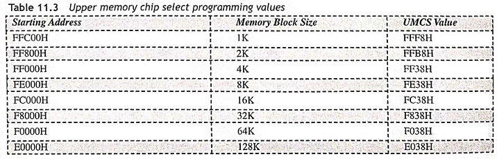
U̅C̅S̅ (Upper Memory CS) The 80186 provides the upper memory chip select signal U̅C̅S̅ to select the top of memory. Generally, the top of memory is used as the system memory as the 80186 starts executing at memory location FFFF0H after reset. The upper limit of memory is represented by the chip select and it is FFFFFH, but the lower limit is programmable. Actually, the lower limit and the size of the select block can be varied by programming as given in Table 11.3.
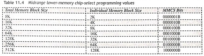
M̅C̅S̅ (Mid-range Memory C̅S̅) The 80186 provides four midrange memory chip select signals which are active within a user locatable memory. This memory block may be within 1 Mbyte memory address space exclusive the area defined by upper-memory chip-select block and lower-memory chip-select block. The base address and the sum of the select memory block for programming are shown in Table 11.4.
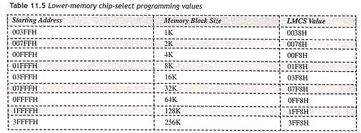
L̅C̅S̅ (Lower Memory) The 80186 provides the lower-memory chip-select signal L̅C̅S̅ to select the bottom of memory. Usually, the bottom of memory is used as the interrupt vector table starting from memory location 00000H. The lower limit of memory is always defined by this chip select and it is 0H. The upper limit and the size of the select memory block can be defined by programming as given in Table 11.5.
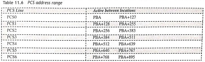
Peripheral Chip Selects ln general, the 80186 generates chip-select signals for up to seven peripheral devices. These chip selects are active for seven adjacent blocks of 128 bytes above a programmable base address. This base address can be located in either memory or I/O space. The 80186 generates seven C̅S̅ lines called P̅C̅S̅0-6. The base address is user-programmable but it will be a multiple of 1 k bytes. Therefore, the least significant 10 bits of the starting address are always 0.
Usually P̅C̅S̅5 and P̅C̅S̅6 are programmed to provide latched address bits A1, A2. If these signals are programmed, they cannot be used as peripheral selects. These outputs can be connected directly to the A0, A1 pins and are used to select internal registers of 8-hit peripheral chips. Then the hardware interface becomes simplified as the 8-bit registers of peripherals are simply treated as 16-bit registers located on even boundaries in I/O or memory space. In this case the lower 8-bits of the register are significant, but the upper 8-bits are ‘don’t cares’
The starting address of the peripheral chip-select block can be described by the Peripheral Chip-Select (PACS) register. This register is located at offset A4H in the internal control block. Bits 15-6 of this register correspond to bits 19-10 of the 20-bit Programmable Base Address (PBA) of the peripheral chip-select block. Bits 9-0 of the PBA of the peripheral chip-select block are all zeros. If the chip-select block is located in I/O space. bits 12-15 must be programmed zero, since the I/O address is only 16 bits wide. Table 11.6 shows the address range of each peripheral chip select with respect to the PBA contained in PACS register.