Architecture of 80486 Microprocessor:
The 80486DX is a 32-bit processor. Figure 11.46 shows the simplified block diagram of 80486 and the internal architecture of 80486 Microprocessor is depicted in Fig. 11.47.
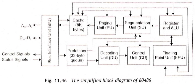
The architecture of Intel’s 80486 can be divided into three different sections such as
- Bus interface unit (BIU),
- Execution and control unit (EU), and
- Floating-point unit (FU).
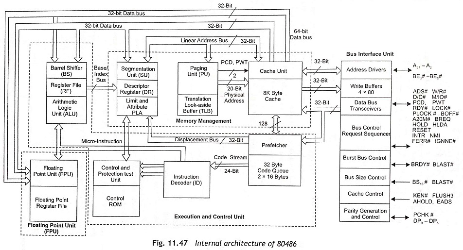
Bus Interface Unit (BIU) The bus interface unit is used to organize all the bus activities of the processor. The address driver is connected with the internal 32-bit address output of the cache and the system bus. The data bus transreceivers are interconnected between the internal 32-bit data bus and system bus. The write data buffer is a queue of four 80-bit registers and is able to hold the 80-bit data which will he written to the memory. Due to pipelined execution of the write operation, data must be available in advance. To control the bus access and operations, the following bus control and request sequencer signals A̅D̅S̅, W/R̅, D/C̅, M/I̅O̅, PCD, PWT, R̅D̅Y̅, L̅O̅C̅K̅, P̅L̅O̅C̅K̅, B̅O̅F̅F̅, A̅2̅0̅M̅, BREQ, HOLD, HLDA, RESET, INTR, NMI, F̅E̅R̅R̅ and I̅G̅N̅N̅E̅ are used.
Execution Unit (EU) and Control Unit (CU) The burst control signal updates the processor that the burst is ready. This signal works as a ready signal in the burst cycle. The B̅L̅A̅S̅T̅ output shows that the previous burst cycle is over. The bus size control signals B̅S̅1̅6̅ and B̅S̅8̅ indicates dynamic bus sizing. The cache control signals K̅E̅N̅, FLUSH, AHOLD and E̅A̅D̅S̅ are used to control the cache control unit.
The parity generation and control unit generates the parity and carries out the checking during the processor operation. The boundary scan control unit of the processor performs boundary scan tests operation to ensure the correct operation of all components of the circuit on the mother board.
The prefetcher unit fetches the codes from the memory and arranges them in a 32-byte code queue. The function of the instruction decoder is to receive the code from the code queue and then decodes the instruction code sequentially. The output of the decoder is fed to the control unit to derive the control signals, which are used for execution of the decoded instructions. Before execution, the protection unit should check all protection norms. If there is in any violation, an appropriate exception is generated.
The control ROM stores a microprogram to generate control signals for execution of instructions. The register hank and ALU are used for their usual operation just like they perform in 80286. The barrel shifter is used to perform the shift and rotate algorithms. The segmentation unit, descriptor registers, paging unit, translation look aside buffer and limit and attribute PLA are worked together for the virtual memory management. These units also provide protection to the op-codes or operand in the physical memory.
Floating–point Unit (FPU) The floating-point unit and register banks or FPU communicate with the bus interface unit (BIU) under the control of memory management unit (MMU), through a 64-bit internal data bus. Generally, the FPU is used for mathematical data processing at very high speed as compared to the ALU.
Flag Register of 80486
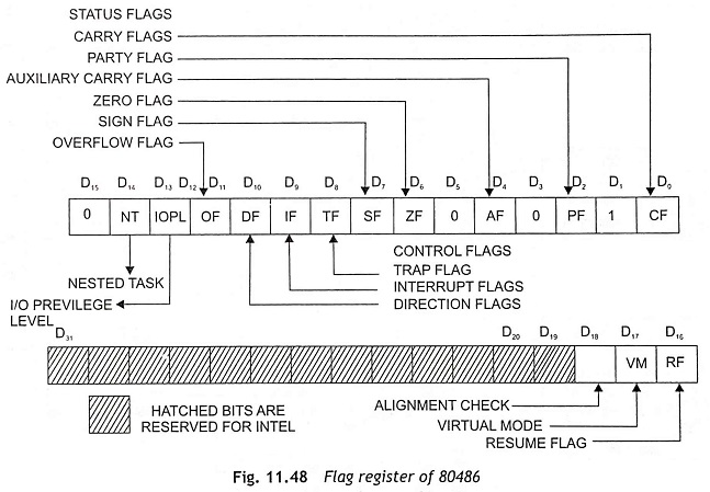
The registers of the 80486 processor are same as the 80386 processor, except for the flag register. Figure 11.48 shows the flag register. As compared to the flag register of 80386, the flag register of 80386 has only one additional flag called alignment check flag or AC flag. The D18 position of the flag register is AC flag as depicted in Fig. 11.48. When the AC flag bit is set to ‘1’, there is an access to a misaligned address and an exception (fault) will be generated. The alignment faults are generated only at privilege level 3.