Architecture of 80286 Microprocessor:
The Architecture of 80286 Microprocessor is an advanced, high-performance microprocessor with specially optimized capabilities for multi-user and multitasking systems. The 80286 has built-in memory protection that supports operating system and task isolation as well as program and data privacy. A 12 MHz 80286 provides about six times more than the 5 MHz 8086. The 80286 includes memory management capabilities that map 230 (one gigabyte) of virtual address space per task into 224 bytes (16 megabytes) of physical memory.
The 80286 is compatible with 8086 and 8088 operating software. The Architecture of 80286 Microprocessor has two operating modes: real address mode and protected virtual address mode. In real address mode, the 80286 is object code compatible with existing 8086, and 8088 software. In protected virtual address mode, the 80286 is source code compatible with 8086, 8088 software and sometimes it may require upgrading to use virtual addresses supported by the 80286’s integrated memory management and protection scheme. Both modes operate at full 80286 performances and execute all instructions of the 8086 and 8088 processors.
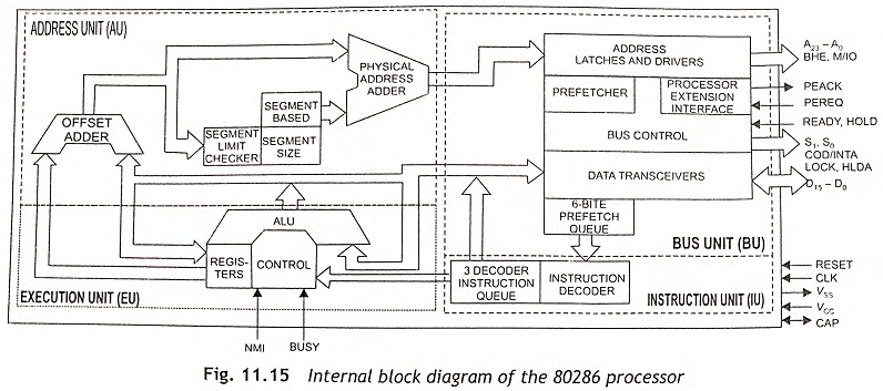
The internal block diagram of the Architecture of 80286 Microprocessor is depicted in Fig. 11.15. The CPU of the 80286 processor consists of four functional units such as
- Address Unit (AU)
- Bus Unit (BU)
- Instruction Unit (IU)
- Execution Unit (EU)
Address Unit (AU) The address unit (AU) is used to determine the physical addresses of instructions and operands which are stored in memory. The AU computes the 20-bit physical address based on the contents of the segment register and 16-bit offset just like 8086. The address lines derived by AU can be used to address different peripheral devices such as memory and I/O devices. This physical address computed by the address unit is sent to the Bus Unit (BU) of the CPU.
Bus Unit (BU) The bus unit interfaces the 80286 with memory and I/O devices. This processor has a 16-bit data bus, a 24-bit address bus, and a control bus. The bus unit is responsible for performing all external bus operations. This unit consists of latches and drivers for the address bus, which transmit the physical address A19-A0. The A19-A0 facilitates all memory and I/O devices for read and write operations.
The bus unit is used to fetch instruction bytes from the memory. Generally, the instructions are fetched in advance and stored in a queue for faster execution of the instructions. This concept is known as instruction pipelining.
Hence, to fetch instruction, the CPU will not wait till the completion of execution of the previous instruction. While one instruction is being executed, the subsequent instruction is to be prefetched, decoded and kept ready for execution. The prefetcher module in the bus unit performs this task of prefetching. The bus unit has a bus control module which controls the prefetcher module. The fetched instructions are arranged in a 6-byte prefetch queue. In this way, the CPU prefetches the instructions, to enhance the speed of execution.
Instruction Unit (IU) The 6-byte prefetch queue forwards the instructions sequentially to the Instruction Unit (IU). The instruction unit receives instructions from the prefetch queue and an instruction decoder decodes them one by one. The decoded instructions are latched onto a decoded instruction queue. The IU decodes maximum 3 prefetched instructions and loads them into decoded instruction queue for execution by execution unit.
Execution Unit (EU) The output of the decoded instruction queue is fed to a control circuit of the execution unit. This unit is responsible for executing the instructions received from the decoded instruction queue. The execution unit consists of the register bank, arithmetic and logic unit (ALU) and control block. The register bank is used for storing the data as a scratch pad. The register hank can also be used as special-purpose registers. The ALU is the core of the EU. and perform all the arithmetic and logical operations and sends the results either over the data bus or back to the register bank. The control block controls the overall operation of the execution unit.
The 80286 CPU family contains all the basic set of registers, instructions, and addressing modes of 8086. The 80286 processor is upward compatible with the 8086, 8088, and 80186 CPU’s. In this section, operations of registers are explained elaborately.
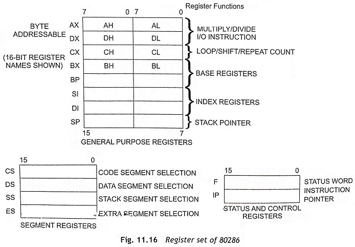
The Architecture of 80286 Microprocessor has fifteen registers as depicted in Fig. 11.16. These registers can he grouped into the four categories as given below:
- General-purpose registers
- Segment registers
- Base and index registers
- Status and control registers
General-Purpose Registers Eight 16-bit general-purpose registers are used to store arithmetic and logical operands. Four of these (AX, BX, CX, and DX) can be used either as 16-bit words or split into pairs of separate 8-bit registers.
Segment Registers Four 16-bit special-purpose registers are used to select the segments of memory that are immediately addressable for code, stack, and data.
Base and Index Registers Four of the general-purpose registers can also be used to determine offset addresses of operands in memory. Usually, these registers hold base addresses or indexes to particular locations within a segment. Any specified addressing mode determines the specific registers used for operand address calculations.
Status and Control Registers The three 16-bit special-purpose registers are used of record and control of the 80286 processor. The instruction pointer contains the offset address of the next sequential instruction to be executed.
Flags Word Description The flags word register records the specific characteristics of the result of arithmetic and logical instructions. The flag register bits D0, D2, D4, D6, D7, and D11 are modified as per result of the execution of arithmetic and logical instructions. These are called status flag hits. Bits D8 and D9 control the operation of the 80286 within a given operating mode and these bits are called control flags. The flag register is a 16-bit register. Figure 11.17 shows the flag register of 80286 and the function of the flag bits are explained below:
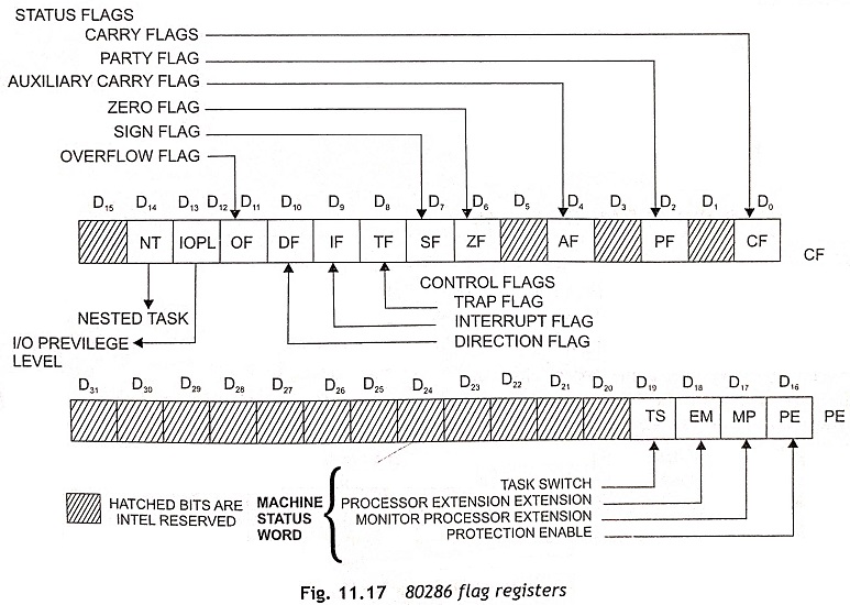
CF Carry Flag (bit D0) Set on high-order bit carry or borrow; cleared otherwise.
PF Parity Flag (bit D2) Set if low-order 8 bits of result contain an even number of 1 bit; cleared otherwise.
AF (bit D4) Set on carry from or borrow to the lower order four bits of AL; cleared otherwise.
ZF Zero Flag (bit D6) Set if result is zero: cleared otherwise,
SF Sign Flag (bit D7) Set equal to high-order bit of result (0 if positive, 1 if negative).
TF Single Step Flag (bit D8) Once set, a single-step interrupt occurs after the next instruction executes. TF is cleared by the single step interrupt.
IF Interrupt–enable Flag (bit D9) When set, maskable interrupts will cause the CPU to transfer control to an interrupt vector specified location.
DF Direction Flag (bit D10) Causes string instructions to auto-decrement the appropriate index registers when set. Clearing DF causes auto increment.
OF Overflow Flag (bit D11) Set if result is a too-large positive number or a too-small negative number (excluding sign-bit) to fit in destination operand: cleared otherwise.
PE (bit D16) Protection enable flag places the 80286 in protected mode, when PE is set. This can only he cleared by resetting the CPU.
MP (bit D17) When MP is set. the monitor processor extension flag allows WAIT instruction to generate a processor extension not present in the exception, i.e., exception number 7.
EM (bit D18) If EM is set, the emulate processor extension nag causes a processor extension absent exception and permits the emulation of processor extension by CPU.
TS (bit D19) When TS set, this flag indicates the next instruction using extension will generate exception 7, permitting the CPU to test whether the current processor extension is for the current task.
Machine Status Word (MSW) The machine status word consists of four flags such as PE, MP, EM and TS of the four lower-order bits D16 to D19 of the upper word or the flag register. The LMSW and SMSW instructions are available in the instruction set of 80286 and these instructions are used to read and write the MSW in real address mode.