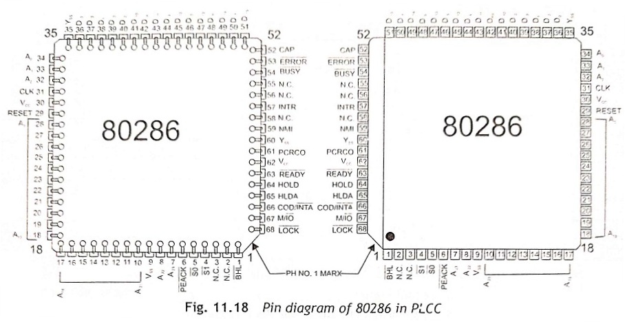
Pin Diagram of 80286 Microprocessor:
The Pin Diagram of 80286 Microprocessor is available in 68-pin PLCC (Plastic Leaded Chip Carrier), 68-pin Ceramic LCC (Lead Less Chip Carrier) and 68-pin PGA (Pin Grid Array) packages. In PLCC, conducting leads are provided for external connections but in LCC, only conducting pads are provided in place of each pin. The Pin Diagram of 80286 Microprocessor for PLCC packages is depicted in Fig. 11.18. The pin functions of 80286 Microprocessor are briefly discussed below:
CLK (I) The CLK is the system clock input pin. The system clock frequency applied at this pin is divided by two inside the 80286 to generate the processor clock. The internal divide-by-two circuits must he synchronized with the external clock generator. The clock is generated using 82284 clock generator.
D15-D0 (I/O) These are sixteen bidirectional data bus lines. The data bus inputs data during memory I/O and interrupt acknowledge read cycles. The data bus Outputs data during memory and I/O write cycles. The data bus is active high and floats to 3-state off during bus hold acknowledge,
A23-A0 (O) These are the physical address output lines used to address memory or I/O port address or I/O devices. A23-A16 are low during I/O transfers. A0 is low when data is to he transferred on pins D7-D0. The address bus is active high and floats to tri-state off during bus hold acknowledge.
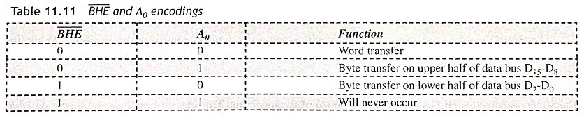
B̅H̅E̅ (O) The bus high enable is an output signal and indicates that there is a transfer on the higher byte of the data bus (D15-D8). Eight-bit oriented devices assigned to the upper byte of the data bus normally use B̅H̅E̅, which is active low and floats to 3-state off during bus hold acknowledge.
S̅0̅, S̅0̅ (O) These are bus cycle status signals. These signals are the active-low status output signals which indicate initiation of a bus cycle. Along with M/I̅O̅ and COD/I̅N̅T̅A̅, these signals define the type of the bus cycle as shown in Table 1 1.12.
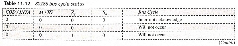
MI I̅O̅ (O) The memory I/O select output signal differentiates memory operations from I/O operations. If this signal is “1”, a memory cycle or a halt/shutdown cycle is in progress. If it is “0”, an I/O cycle or interrupt acknowledge cycle is in progress.
COD / I̅N̅T̅A̅ (O) The code/interrupt acknowledges output signal distinguishes instruction fetch cycle from memory data read cycles. This signal also differentiates interrupt acknowledge cycles from I/O cycles.
L̅O̅C̅K̅ (O) This active-low output signal is used to indicate that the other system masters are not to fain control of the system bus for the current and the following bus cycles. This signal is activated by L̅O̅C̅K̅ instruction prefix, or automatically by hardware during XCHG, interrupt acknowledge or descriptor table access. L̅O̅C̅K̅ is active low and floats to 3-state off during bus hold acknowledge.
R̅E̅A̅D̅Y̅ (I) This is an active-low input signal. It is used to terminate a bus cycle. Bus cycles are extended without limit until terminated by R̅E̅A̅D̅Y̅ low. This signal is neglected during HLDA cycle.
HOLD and HLDA The hold request (HOLD) and hold acknowledge (HLDA) control ownership of the local bus of 80286.
The HOLD input signal allows another local bus master to request control of the local bus. While the control is granted, the 80286 will float its bus drivers to 3-state off and then activate the hold acknowledge (HLDA) signal.
The local bus must be remain granted to the requesting master until HOLD becomes inactive so that the 80286 deactivates HLDA and regains control of the local bus. This can terminate the hold acknowledge condition. These signals are active high.
INTR (I) The interrupt request (INTR) signal requests the 80286 to suspend the execution of current instruction and provide service to a pending interrupt request. Its function is just like that of INTR pin of 8086.
Whenever the interrupt enable bit in the flag word is cleared, interrupt requests are masked. When the 80286 responds to an interrupt request, it performs two interrupt acknowledge bus cycles to read an 8-hit interrupt vector. INTR is active high and may he asynchronous to the system clock.
NMI (I) The non-maskable interrupt (NMI) request is an active-high, edge-triggered input signal. This signal interrupts the 80286 with an internally supplied vector value of 2. No acknowledge cycles are needed to be carried out. For proper recognition of NMI, this input signal must be previous low for at least four system clock cycles and remain high fir at least four system clock cycles,
PEREQ (I) and P̅E̅A̅C̅K̅ (O) The processor extension request and acknowledgement (PEREQ) and acknowledge (P̅E̅A̅C̅K̅) extend the memory management and protection capabilities of the 80286 to coprocessor (80287 in case of 80286 CPU).
The PEREQ input requests the 80286 to perform a data-operand transfer for a processor extension, The P̅E̅A̅C̅K̅ is an active-low output signal that indicates to the processor extension that the requested operand is being transferred.
B̅U̅S̅Y̅ (I) and E̅R̅R̅O̅R̅ (I) The processor extension busy (B̅U̅S̅Y̅) and error (E̅R̅R̅O̅R̅) arc active-low input signals that indicate the operating conditions of a processor extension to 80286. When the B̅U̅S̅Y̅ becomes low, 80286 stops the program execution and waits until the B̅U̅S̅Y̅ becomes inactive. During this time, the processor extension is busy with its allotted job, After completion of the job, the processor extension drives the B̅U̅S̅Y̅ input high indicating 80286 to continue with the program execution. An active E̅R̅R̅O̅R̅ input signal causes the 80286 to perform the processor extension interrupt while executing the WAIT or ESC instructions.
CAP (I) A substrate filter capacitor, 0.047 μf, 12 V must be connected between this input pin and ground to filter the output of the internal substrate bias generator. For correct operation of 80286 the capacitor must be charged to its operating voltage. Till this capacitor charges to its full capacity, the 80286 may be kept stuck to reset to avoid any spurious activity. A maximum dc leakage current of 1 μA is allowed through the capacitor.
Vss (I) This pin is ground at 0 volts.
VCC (I) This pin is used to apply + 5 V power supply voltage of 80286.
RESET (I) The system RESET input clears the internal logic of 80286, and it is active high. Due to a low to high transition on RESET, the 80286 may be reinitialized. For proper reinitialize, the active-high reset input pulse width should be at least 16 clock cycles.