Pin Diagram of 8087 Processor:
Figure 7.46 shows the pin diagram of 8087 processor. The operations of all pins of 8087 are explained below:
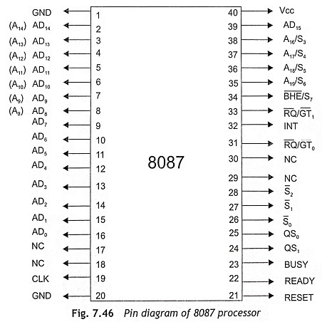
AD15-AD0 The AD15-AD0 are the time multiplexed address/data lines. During T1, these lines are used as address bus A15-A0 and these lines can be used as data bus D15-D0 during T2, T3, Tw and T4 states. A0 is also used as the chip select signal whenever the data transfer is on lower byte (D7-D0) of data bus.
A19/S6-A16/S3 These lines are the time-multiplexed address/status lines and their function are same as the corresponding pins of 8086. The S6, S4 and S3 are high, when the S5 is low.
B̅H̅E̅/S7 The B̅H̅E̅/S7 pin is used to select data on the higher byte of the 8086 data bus during T1. During T2, T3, Tw and T4 , this signal is a status line S7.
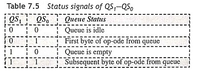
QS1-QS0 The queue status input signals, QS1 and QS0 are used to allow the co-processor to track the progress of an instruction through the 8086 queue and help 8087 co-processor to determine when to access the bus for the escape opcode and operand. These signals can also maintain synchronism with main CPU and indicate the status of the internal instruction queue as given in the Table 7.5.
INT The interrupt output signal INT is used by 8087 to indicate an unmasked exception that has been received during execution. Usually this signal is handled by 8259A programmable interrupt controller.
BUSY The BUSY output signal is used to indicate to the CPU that 8087 co-processor is busy with the execution of an allotted instruction.
READY The READY input signal can be used to indicate the 8087 co-processor that the addressed device has completed the data transfer and the bus becomes free for the next bus cycle. Usually, this signal is synchronized by the clock generator 8284.
RESET This input signal is used to rest the co-processor after escaping the all internal activities and is ready for execution of any instruction send by the main processor.
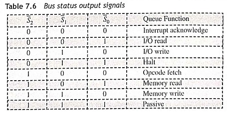
S2, S1 and S0 These lines are bus status output signals that encode the type of the current bus cycle as given in Table 7.6.
RQ/GT0 The bus request/grant output signal RQ/GT0 is used by the 8087 to control of the bus from the host 8086/8088 for operand transfers. This pin must be connected to the request/grant pin of the host processor.
RQ/GT1 The RQ/GT1 bidirectional pin is used by the other bus masters like DMA controllers to convey their need of the local bus access to 8087. This request must be further conveyed to the host processor.
CLK The input clock signal CLK provides the basic timings for the co-processor operation.
VCC This is a +5 V supply line which is used for the circuit operation.
GND This Pin Diagram of 8087 Processor is connected with the ground terminal of the power supply.