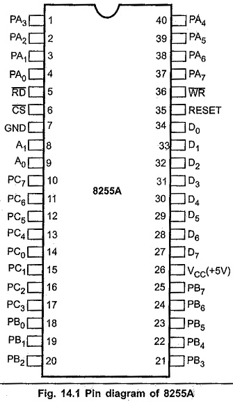
8255 Pin Diagram:
Fig. 14.1 shows the 8255 Pin Diagram of Microprocessor.
8255 Block Diagram:
Fig. 14.2 shows the internal 8255 block diagram of 8255 Pin Diagram Microprocessor. It consists of data bus buffer, control logic and Group A and Group B controls.
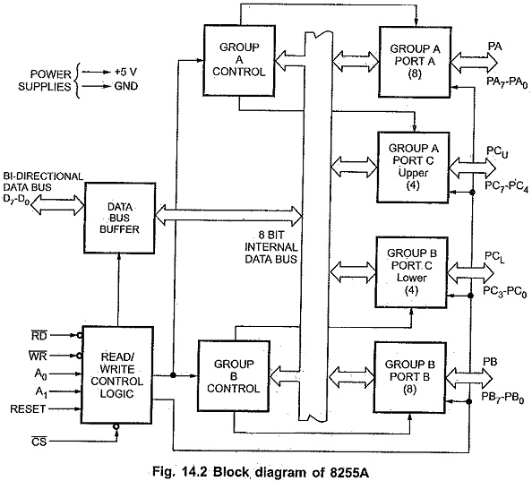
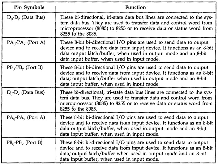
Data Bus Buffer:
This tri-state bi-directional buffer is used to interface the internal data bus of 8255 Pin Diagram to the system data bus. Input or Output instructions executed by the CPU either Read data from, or Write data into the buffer. Output data from the CPU to the ports or control register, and input data to the CPU from the ports or status register are all passed through the buffer.
Control Logic:
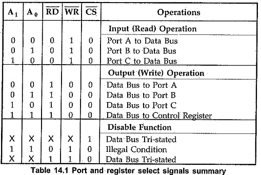
The control logic block accepts control bus signals as well as inputs from the address bus, and issues commands to the individual group control blocks (Group A control and Group B control). It issues appropriate enabling signals to access the required data/control words or status word. The input pins for the control logic section are described here.
Group A and Group B Controls:
Each of the Group A and Group B control blocks receives control words from the CPU and issues appropriate commands to the ports associated with it. The Group A control block controls Port A and PC7-PC4 while the Group B control block controls Port B and PC3-PC0.
Port A :
This has an 8-bit latched and buffered output and an 8-bit input latch. It can be programmed in three modes: mode 0, mode 1 and mode 2.
Port B :
This has an 8-bit data I/O latch/ buffer and an 8-bit data input buffer. It can be programmed in mode 0 and mode 1.
Port C :
This has one 8-bit unlatched input buffer and an 8-bit output latch/buffer. Port C can be splitted into two parts and each can be used as control signals for ports A and B in the handshake mode. It can be programmed for bit set/reset operation.
Modes of Operation of 8255 Microprocessor:
Bit Set-Reset (BSR) Mode:
The individual bits of Port C can be set or reset by sending out a single OUT instruction to the control register. When Port C is used for control/status operation, this feature can be used to set or reset individual bits.
I/O Modes:
Mode 0 : Simple input/output:
In this mode, ports A and B are used as two simple 8-bit I/O ports and Port C as two 4-bit ports. Each port (or half – port, in case of C) can be programmed to function as simply an input port or an output port. The input/output features in Mode 0 are as follows :
- Outputs are latched.
- 2. Inputs are buffered, not latched.
- Ports do not have handshake or interrupt capability.
Mode 1 : Input/Output with handshake:
In this mode, input or output data transfer is controlled by handshaking signals. Handshaking signals are used to transfer data between devices . whose data transfer speeds are not same. For example, computer can send data .to the printer with large speed but printer can’t accept data and print data with this rate. So computer has to send data with the speed with which printer can accept. This type of data transfer is achieved by using handshaking signals along-with data signals. Fig. 14.3 shows data transfer between computer and printer using handshaking signals.
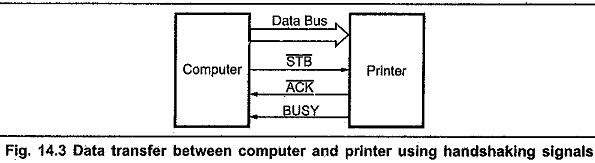
These handshaking signals are used to tell computer whether printer is ready to accept the data or not. If printer is ready to accept the data then after sending data on data bus, computer uses another handshaking signal (STB) to tell printer that valid data is available on the data bus.
The 8255 Pin Diagram mode 1 which supports handshaking has following features.
- Two ports (A and B) function as 8-bit I/O ports. They, can be configured either as input or output ports.
- Each port uses three lines from Port C as handshake signals. The remaining two lines of. Port C can be used for simple I/O functions.
- Input and output data are latched.
- Interrupt logic is supported.
- Mode 2 : Bi-directional I/O data transfer:
This mode allows bi-directional data transfer (transmission and reception) over a single 8-bit data bus using handshaking signals. This feature is available only in Group A with Port A as the 8-bit bidirectional data bus; and PC3 – PC7 are used for handshaking purpose. In this mode, both inputs and outputs are latched. Due to use of a single 8-bit data bus for bi-directional data transfer, the data sent out by the CPU through Port A appears on the bus connecting it to the peripheral, only when the peripheral requests it. The remaining lines of Port C i.e. PC0-PC2 can be used for simple I/O functions. The Port B can be programmed in mode 0 or in mode 1. When Port B is programmed in mode 1, PC0-PC2 lines of Port C are used as handshaking signals.
Control Word Formats:
A high on the RESET pin causes all 24 lines of the three 8-bit ports to be in the input mode. All flip-flops are cleared and the interrupts are reset. This condition is maintained even after the RESET goes low. The ports of the 8255 Pin Diagram can then be programmed for any other mode by writing a single control word into the control register, when required.
For Bit Set/Reset Mode:
Fig. 14.4 shows bit set/reset control word format.
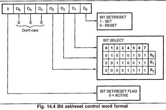
The eight possible combinations of the states of bits D3 – D1 (B2 B1 B0) in the Bit Set-Reset format (BSR) determine particular bit in PC0 – PC7 being set or reset as per the status of bit D0. A BSR word is to be written for each bit that is to be set or reset. For example, if bit PC3 is to be set and bit PC4 is to be reset, the appropriate BSR words that will have to be loaded into the control register will be, 0XXX0111 and 0XXX1000, respectively, where x is don’t care.
The BSR word can also be used for enabling or disabling interrupt signals generated by Port C when the 8255 Pin Diagram is programmed for Mode 1 or 2 operation. This is done by setting or resetting the associated bits of the interrupts. This is described in detail in next section.
For I/O Mode:
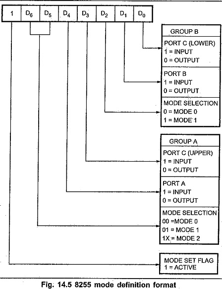
The mode definition format for I/O mode is shown in Fig. 14.5. The control words for both, mode definition and Bit Set –Reset are loaded into the same control register, with bit D7 used for specifying whether the word loaded into the control register is a mode definition word or Bit Set-Reset word. If D7 is high, the word is taken as a mode definition word, and if it is low, it is taken as a Bit Set-Reset word. The appropriate bits are set or reset depending on the type of operation desired, and loaded into the control register.