Intel 80386 Pin Diagram Description:
The 80286 family has a sinking current of 2.0 mA but each output pin of the 80386 is capable of sinking 4.0 mA current for address and data buses or 5.0 mA for other connections. Therefore, there is significant improvement in the current handling capability. Figure 11.36 shows the Intel 80386 Pin Diagram Description.
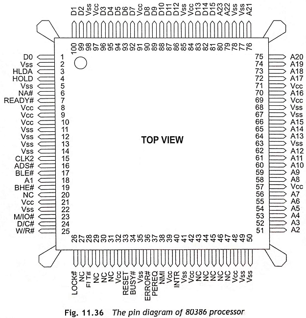
A31-A2 (Address Bus) Address lines A31-A2 are used as the upper 30 bits of the 32-bit address bus. These lines can address any memory locations of 1 GB x 32 memory in the 80386 memory system.
A1-A0 A1 and A0 are encoded to generate BE3, BE2, BE1 and BE0.
D31-D0 (Data Bus) The data bus D31-D0 are used to transfer data between the microprocessor and memory and input/output devices.
BE3–BE0 (Bank Enable Signals) The memory system of 80386 can he observed as a 4-byte wide memory access mechanism. The four byte enable signals arc BE3, BE2, BE1 and BE0. These signals are used to enable four banks. These signals are generated by the microprocessor from address bits A1 and A0 and used to access 1 byte, 2 bytes or word and 4bytes or double word of data simultaneously.
M/I̅O̅ (Memory/Input/Output) The M/I̅O̅ pin is used to select the memory and I/O related operations. When it is logic level ‘1’, memory devices will be selected. If it is logic level ‘0’, I/O devices will be selected for data transfer. During I/O operation, the address bus consists of a 16-bit I/O address.
W/R̅ (Write/Read) The W/R̅ signal is used to indicate the read and write bus cycles. When W/R̅ =1, the current bus cycle is a write cycle. If W/R̅ = 0, the current bus cycle is a read cycle.
A̅D̅S̅ (Address Data Strobe) This 80386 Pin Diagram issues a valid memory or I/O address and the address bus and bus cycle pins W/R̅, D/C̅, M/I̅O̅ and BE3-BE0 are holding their respective valid signals.
RESET When RESET pin is high, the processor suspends the current operation and becomes reset. Therefore, the processor restarts the execution from the starting memory location FFFFFFF0H.
CLK2 (Clock time 2) The CLK2 input pin provides a clock signal for the operation of 80386 and the clock frequency is two times of the operating frequency of the 80386.
R̅E̅A̅D̅Y̅ The R̅E̅A̅D̅Y̅ signal indicates that the previous bus cycle has been completed and the bus is ready for the next bus cycle. This signal controls the number of WAIT states inserted into the bus cycle. Usually, this signal is used for interfacing slow I/O devices with CPU.
L̅O̅C̅K̅ When the L̅O̅C̅K̅ output pin is at logic level 0, the bus lock prevents the other bus masters from gaining control of the system bus. This signal is most frequently used during DMA accesses.
D/C̅ (Data and Control) The D/C̅ output signal indicates whether the current bus cycle is data cycle, i.e., memory and I/O read or write cycles, or the current bus cycle is a control cycle, i.e., interrupt acknowledge, halt or code fetch operations.
BS16 Bus size of 16 bits BS16 indicates the interfacing of 16-bit devices with the 32-bit wide 80386 data bus.
N̅A̅ The N̅A̅ represents the Next Address input signal. When this signal is active low, it allows address pipelining in the 80386 bus cycles.
HOLD The Hold request signal allows another bus master to request control of the local bus. This signal is commonly used in DMA operation just like it did on the 8086 microprocessor.
HLDA The Hold Acknowledge (HLDA) indicates that the 80386 processor has surrendered control of its local bus to another bus master.
P̅E̅R̅E̅Q̅ The Processor Extension Request (PEREQ) indicates that the 80387 arithmetic coprocessor has data to transfer to the processor.
B̅U̅S̅Y̅ The BUSY input signal indicates that the math coprocessor is busy.
E̅R̅R̅O̅R̅ The Error input signal indicates that the math coprocessor has an error condition.
INTR The Interrupt Request (INTR) pin is used as a maskable interrupt input. This pin will be masked using the IF of the flag register.
NMI The Non-maskable Interrupt (NMI) signal requests a nonmaskable interrupt just like the 8086 microprocessor.
VCC This pin is connected to a +VCC system power supply.
VSS System ground provides the 0 V connection. This pin is connected to a ground terminal of system power supply.