Pin Photodiode – Definition, Working and Applications:
The PIN photodiode is one of the most common photodetectors, since the depletion-region thickness (intrinsic layer) can be tailored to optimize the quantum efficiency and the frequency response. The Pin Photodiode is depicted in Fig. 25.26(a). It consists of a P region and an N region separated by an intrinsic region. The width W of intrinsic region is much larger than the space charge width of an ordinary P-N junction. The ‘I’ region need not be truly intrinsic, as long as the resistivity is high. It can be grown epitaxially on the N-type substrate, and the P-region can be obtained by the implantation.
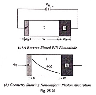
When there is no bias applied to the diode, there will be diffusion of charge carriers due to concentration gradient across the junction. Diffusion holes and electrons across NI junction form a very thin depletion layer in the N-region and a relatively thicker depletion layer in I-region containing equal but opposite fixed charges. When a reverse bias is applied and gradually increased, the thickness of the depletion layer increases until the entire I-region is swept free of mobile carriers. Thus with a reverse bias applied to the PIN diode, the space charge region extends completely through the intrinsic region.
Assume that a photon flux Φo is incident on the P+ region and width WP of P-region is very small. Now the photon flux, as a function of distance, in the intrinsic region is Φ (x) = Φoe-αx where α is the photon absorption coefficient, as depicted in Fig. 25.26(b). The density of photocurrent produced in the intrinsic region can be given by
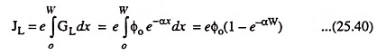
In derivation of above equation it has been assumed that there is no electron-hole recombination within the space charge region and also that each photon absorbed generates one EHP.
Although PN photodiode provides a much high frequency response than CdS bulk-type photoconductor but even faster response may be achieved with the help of PIN photodiode. PIN photodiodes are relatively inexpensive and ultrafast having a switching speed of nanosecond or so and interface easily with conventional electronic circuitry. They have broad spectral response and generate very low noise. They are capable of processing very weak signals.
Hence, such devices are widely employed for detection of laser pulses and in ultrafast switching and logic circuits.