8251 Pin Diagram:
Fig. 14.36 shows the 8251 Pin Diagram.
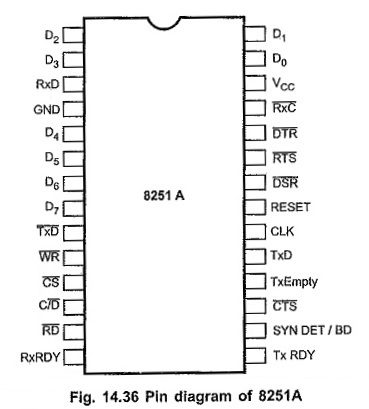
Data Bus : Bi-directional, tri-state, 8-bit Data Bus. This pin allow transfer of bytes between the CPU and the 8251A.
RD (Read) : A low on this input allows the CPU to read data or status bytes from 8251A
WR (Write) : A low on this input allows the CPU to write data or command word to the 8251A.
CLK (Clock) : The CLK input is used to generate internal device timing. The frequency of CLK must be greater than 30 times the receiver or transmitter data bit rates.
RESET : A high on this input forces the 8251A into an “Idle” mode. The device will remain at “Idle” until a new set of control words is written into the 8251 Pin Diagram to program its functional definition.
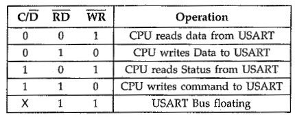
C/D (Control /Data) : This input in conjunction with the WR and RD inputs, informs the 8251A that the word on the Data Bus is either a data character control word or status information as shown in table.
CS (Chip Select) : A low on this input allows communication between CPU and 8251A
Modem Control Signals:
The 8251 Pin Diagram has a set of control inputs and outputs that can be used to simplify the interface to almost any modem.
DSR (Data Set Ready) : This input signal is used to test modem conditions such as Data Set Ready.
DTR (Data Terminal Ready) : This output signal is used to tell modem that Data Terminal is ready.
RTS (Request to Send ) : This output signal is asserted to begin transmission.
CTS (Clear to Send) : A low on this input enables the 8251A to transmit serial data if the TxE bit in the command byte is set to a “one”.
Note : The modem control signals are general purpose in nature and can be used for functions other than modem control, if necessary. The DSR can be used as an inverted input port and DTR can be used as an inverted output port.
Transmitter Signals:
TxD : Transmit data : This output signal outputs a composite serial stream of data on the falling edge of TxC.
TxRDY (Transmitter Ready) : This output signal indicates the CPU that the transmitter is ready to accept a data character.
TxE (Transmitter Empty) : This output signal indicates that the transmitter has no character to transmit.
TxC (Transmitter Clock) : This clock input controls the rate at which the character is to be transmitted.
Receiver Signals:
RxD (Receiver data) : This input receives a composite serial stream of data on the rising edge of RxC.
RxRDY (Receiver Ready) : This output indicates that the 8251 Pin Diagram contains a character that is ready to be input to the CPU.
RxC (Receiver Clock) : This clock input controls the rate at which the character is to be received.
SYNDET (Sync Detect)/ BRKDET (Break Detect):
This pin is used in synchronous mode for detection of synchronous characters and may be used as either input or output.
In asynchronous mode this pin goes high if receiver line stays low for more than 2 character times. It then indicates a break in the data stream.
When used as an input (external sync detect mode) a positive signal will cause the 8251A to start receiving data characters on the rising edge of the next RXC.