8251 Block Diagram in Microprocessor:
Fig. 14.37 shows the 8251 Block Diagram in Microprocessor. It includes : Data bus buffer, Read/Write control logic, modem control, Transmit buffer, Transmit Control, Receiver Buffer and Receiver control.
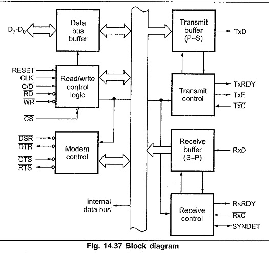
Data Bus Buffer :
This tri-state, bi-directional, 8-bit buffer is used to interface 8251 Block Diagram in Microprocessor to the system data bus. Along with the data, control word, command words and status information are also transferred through the Data Bus Buffer.
Read/Write control logic :
This functional block accepts inputs from the system control bus and generates control signals for overall device operation. It decodes control signals on the 8085 control bus into signals which controls the internal and external I/O bus. It contains the control word register and command word register that stores the various control formats for the device functional definition.
Transmit Buffer:
The transmit buffer accepts parallel data from the CPU, adds the appropriate framing information, serializes it, and transmits it on the TxD pin on the falling edge of TxC.
It has two registers : A buffer register to hold eight bits and an output register to convert eight bits into a stream of serial bits. The CPU writes a byte in the buffer register, Which is transferred to the output register when it is empty. The output register then transmits serial data on the TxD pin.
In the asynchronous mode the transmitter always adds START bit; depending on how the unit is programmed, it also adds an optional even or odd parity bit, and either 1, 1 1/2, or 2 STOP bits. In synchronous mode no extra bits (other than parity, if enable) are generated by the transmitter.
8251 Transmitter Control :
It manages all activities associated with the transmission of serial data. It accepts and issues signals both externally and internally to accomplish this function.
TxRDY (Transmit Ready ) : This output signal indicates CPU that buffer register is empty and the USART is ready to accept a data character. It can be used as an interrupt to the system or, for polled operation, the CPU can ‘check TxRDY using the status read operation. This signal is reset when a data byte is loaded into the bliffer register.
TxE (Transmitter Empty) : This is an output signal. A high on this line indicates that the output buffer is empty. In the synchronous mode, if the CPU has failed to load a new character in time, TxE will go high momentarily as SYN characters are loaded into the transmitter to fill the gap in transmission.
TxC (Transmitter Clock) : This clock controls the rate at which characters are transmitted by USART. In the synchronous mode TxC is equivalent to the ‘baud rate, and is supplied by the modem. In asynchronous mode TxC is 1, 16, or 64 times the baud rate. The clock division is programmable. It can be programmed by writing proper mode word in the mode set register.
Receiver Buffer:
The receiver accepts serial data on the RxD line, converts this serial data to parallel format, checks for bits or characters that are unique to the communication technique and sends an “assembled” character to the CPU.
When 8251 Block Diagram in Microprocessor is in the asynchronous mode an4 it is ready to accept a character, it looks for a low level on the RxD line. When it receives the low level, it assumes that it is a START bit and enables an internal counter, At a count equivalent to one-half of a hit time, the RxD line is sampled again. If the line is still low, a valid START bit is detected and the 8251A proceeds to assemble the character. After successful reception of a START bit the 8251A receives data, parity and STOP bits, and then transfers the data on the receiver input register. The data is then transferred into the receiver buffer register.
In the synchronous mode the receiver simply receives the specified number of data bits and transfers them to the receiver input register and then to the receiver buffer register.
Receiver Control:
It manages all receiver-related activities. Along with data reception, it does false start bit detection, parity error detection, framing error detection, sync detection and break detection.
RxRDY (Receiver Ready) : This is an output signal. It goes high (active), when the USART has a character in the buffer register and is ready to transfer it to the CPU. This line can be used either to indicate the status in the status register or to interrupt the CPU. This signal is reset when a data byte from receiver buffer is read by the CPU.
RxC (Receiver Clock) : This clock controls the rate at which the character is to be received by USART in the synchronous mode. RxC is equivalent to the baud rate, and is supplied by the modem. In asynchronous mode RxC is 1, 16, or 64 times the baud rate. The clock division is programmable. It can be programmed by writing proper mode word in the mode set register.
Modem Control:
The 8251 Block Diagram in Microprocessor has a set of control inputs and output’s that can be used to simplify the interface to almost any modem. It provides control circuitry for the generation of RTS and DTR and the reception of CTS and DSR. In addition, a general purpose inverted output and a general purpose input are provided. The output is labeled DTR and the input is labeled DSR. DTR can be asserted by setting bit 2 of the command instruction; DSR can be sensed as bit 7 of the status register. When used as a modem control signal DTR indicates that the terminal is ready to communicate and DSR indicates that it is ready for communication.
Control Word of 8251:
The Control Word of 8251 defines the complete functional definition of 8251 Block Diagram in Microprocessor and they must be loaded before any transmission or reception. The control words of Block Diagram of 8251 Microcontroller are split into two formats
- Mode instruction
- Command instruction
Mode Instruction :
Fig. 14.38 shows the mode instruction format of 8251.
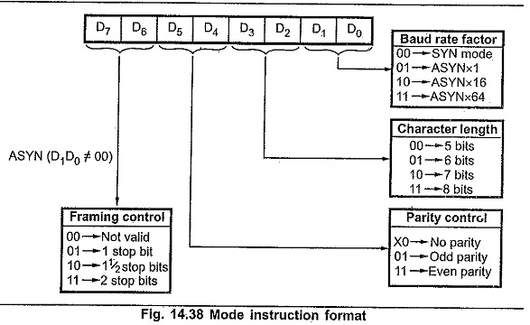
The instruction can be considered as four 2-bit fields. The first 2-bit field (D1-D0) determines whether the USART is to operate in the synchronous (00) or asynchronous mode. In the asychronous mode, this field determines the division factor for clock to decide the baud rate. For example, if D1 and D0 are both ones, the RxC and TxC will be divided by 64 to establish the baud rate.
The second 2-bit field (D3-D2) determines number of data bits in one character. With this 2-bit field we can set character length from 5-bits to 8 bits.
The third 2-bit field, (D5-D4), controls the parity generation. The parity bit is added to the data bits only if parity is enabled.
The last field, (D7-D6), has two meanings depending on whether operation is to be in the synchronous or asynchronous mode. For asynchronous mode, (i.e. D1D0 ≠ 00), it controls the number of STOP bits to be transmitted with the character. In synchronous mode, (i.e. D1D0) = 00) this field controls the synchronizing process. It decides whether to operate with external synchronization or internal synchronization and whether to transmit single synchronizing character or two synchronizing characters.
Command Instruction:
After the mode instruction, command character should be issued to the USART. It controls the operation of the USART within the basic frame work established by the mode instruction. Fig. 14.39 shows command instruction format.
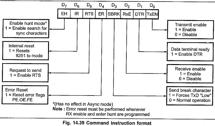
It does function such as : Enable Transmit/Receive; Error Reset and modem Control.
8251A Status Word:
In the data communication systems it is often necessary to examine the “status” of the transmitter and receiver. It is also necessary for CPU to know if any error has occurred during communication. The 8251 Block Diagram in Microprocessor allow the programmer to read above mentioned information from the status register any time during the functional operation. Fig. 14.40 shows the format of status register.
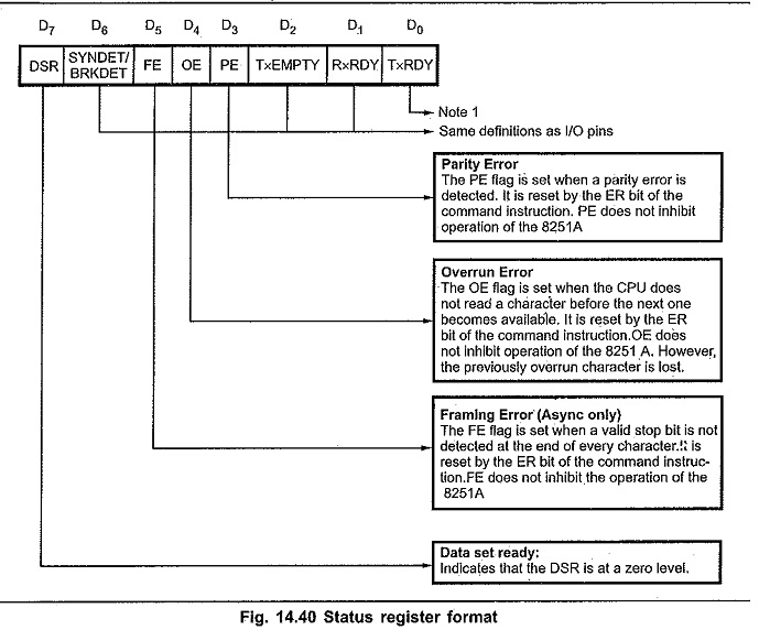
Error Definitions:
Parity Error : At the time of transmission of data an even or odd parity bit is inserted in the data stream. At the receiver end, if parity of the character does not match with the pre-defined parity, parity error occurs.
Overrun Error : In the receiver section received character is stored in the receiver buffer. The CPU is supposed to read this character before reception of the next character. But if CPU fails in reading the character loaded in the receiver buffer, the next the received character replaces the previous one and the OVERRRUN Error occurs.
Framing Error : If valid stop bit is not detected at the end each character framing error occurs.
All these errors, when occur, set the corrosponding bits in the status register. These error bits are reset by setting ER bit in the command instruction.