Color Television Receiver Block Diagram:
Figure 17-25 shows the block diagram of a Color Television Receiver Block Diagram, but for simplicity the circuits shown in Figure 17-23 are omitted. Interconnection points are shown on both diagrams, so that there should be no difficulty in reconciling the two figures. It is now proposed to look first at the (remaining) common circuits in the Color Television Receiver Block Diagram, i.e., those circuits which have direct counterparts in monochrome receivers, commenting on those differences that exist.
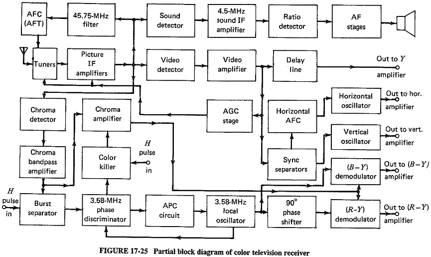
A Color Television Receiver Block Diagram almost invariably has an AFC circuit, as indicated in Figure 17-25. It is often called automatic fine tuning (AFT) and is used automatically to minimize mistuning, particularly to too high a frequency. This would produce added amplification of the sound carrier, and hence 920-kHz interference between the chroma and sound carriers. If the receiver is misadjusted to too low a frequency, insufficient gain will be available in the IF amplifiers at the chroma subcarrier frequency, and the output will be lacking in color. The AFT circuit consists basically of a 45.75-MHz filter, whose output is fed to a phase discriminator. This produces a de correcting voltage whenever its input frequency differs from 45.75 MHz, and this voltage is applied to a varactor diode in the circuit of the appropriate local oscillator in the tuner. It is normally possible to switch out the AFT circuit, so as to permit manual fine tuning.
The next point of difference from monochrome receivers arises in connection with sound demodulation. The intercarrier system is still used, but this time sound is extracted at an earlier point, again to reduce interference between it and chroma. The output of the last IF amplifier is fed to three separate, but more or less identical, diode detectors. Each of these acts as a nonlinear resistance, with the usual difference frequencies appearing in its output. The frequency selected from the output of the sound detector is 4.5 MHz, and this is then followed by exactly the same circuitry as in a monochrome receiver.
The output of the video detector undergoes the same treatment as in black-and-white receivers, with two differences. The first of these is that additional sound traps are provided, and the bandwidth of the video amplifiers is somewhat narrower than in a monochrome receiver. The other is to reduce interference between the Y signal, which these amplifiers handle, and the lowest I sidebands of the chroma signal. The second difference is denoted by the presence of the delay line in. Figure 17-25. It will be recalled that the Y signal is subtracted from R, G and B in or just before the picture, so that a correct phase relation there is essential. In the next section, the chroma signal undergoes more phase delay than the luminance signal before reaching the picture tube, and so a correction is required. The simplest method of equalizing the phase differences is by introducing a delay into the Y channel. This delay is normally just under 1 μs.
Color Circuits:
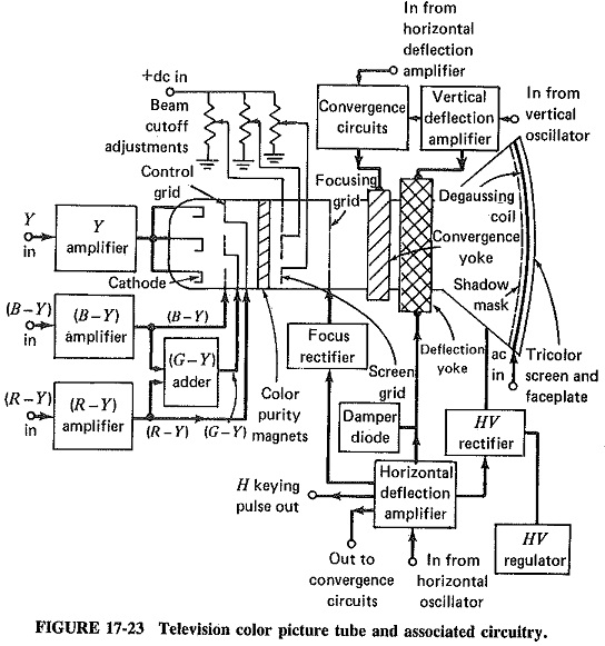
We have reached the stage where we know how the luminance signal is delivered to the cathode of the picture tube, and the sound signal to the loudspeaker. We also know what deflection currents are required, and how they are obtained. We know what other inputs the picture tube requires and at what point the chroma subcarrier is divorced from the luminance voltages. What we must now do is to determine what happens in the circuitry between the chroma takeoff point and the (B — Y) and (R — Y) inputs to the appropriate amplifiers preceding the picture tube grids in Figure 17-23.
The output of the chroma detector is fed to a bandpass amplifier, having a frequency response designed to reject the lower video frequencies representing Y signals, as well as the 4.5-MHz sound carrier. In more elaborate receivers the bandpass stretches from 1.5 MHz below to 0.5 MHz above the 3.58-MHz chroma subcarrier. In most Color Television Receiver Block Diagram this bandpass is only 3.58 ± 0.5 MHz, so that some of the transmitted I information is lost. The resulting loss in color definition is not too serious, and the advantage is a reduction in interference from the distant Y sidebands. The use of this arrangement is widespread. The chroma signal is now amplified again and fed to the color demodulators. Because the chroma amplifiers have a much narrower bandwidth than the Y video amplifiers, a greater phase delay is introduced here hence the delay line used in the Y channel.
It was shown in the preceding section that two color signals, such as (B — Y) and (R — Y), are sufficient, because the third one can be obtained from them by vector addition. It is necessary to decide which two color signals should be obtained, by the appropriate demodulation of the chroma output. At first sight, it would seem obvious that the two signals should be I and Q, for which R, G and B would be obtained by a matrixing process that is likely to be the reverse. This is rather awkward to do and requires sufficient bandwidth to make all of the I signal available in the first place an unlikely situation. The next logical thought is to try to obtain the R, G and B signals directly, but this is also awkward, because the required phase differences between these three vectors and the reference burst (77°, 299° and 193°) are also difficult to produce.
The result of the foregoing considerations is that most Color Television Receiver Block Diagram produce the (R — Y) and (B — Y) voltages from their color demodulators. This results in the loss of a little color information, but this loss is outweighed by two important considerations. The first is the easy production of the requisite phase differences with respect to the color burst, being 90° for (R — Y) and 180° for (B — Y). The second reason for using this arrangement is that the resulting signals can be matrixed by the picture tube without any further processing.
Synchronous demodulators are used for detecting the (R — Y) and (B — Y) signals. As shown in the block diagram of Figure 17-25, each such detector has two input signals. The chroma which it is required to demodulate and the output of the local 3.58-MHz crystal oscillator. The second signal is used to gate the detector, producing the correct output when the chroma signal is in phase with the local oscillator. If the phase of the local oscillator corresponds to the (B — Y) vector, the demodulated voltages will also be (B — Y). As in the other color demodulator of Figure 17-25, a 90° phase change is introduced into the 3.58-MHz oscillator signal, its phase will now correspond to that of the (R — Y) vector, and (R — Y) chroma voltages will be the only ones produced. In this fashion, the 90° phase difference between the two sets of voltages is used to separate them in the outputs of their respective demodulators.
The burst separator has the function of extracting the 8 to 11 cycles of reference color burst which are transmitted on the back porch of every horizontal sync pulse. This is done by having an amplifier biased so that only signals having amplitudes corresponding to the burst level (or higher) are passed. This amplifier is capable of amplifying only during the back porch, so that only the burst information is amplified. This is achieved by keying it with pulses derived from the horizontal output stage. The situation then is that the burst separator will amplify only when such a keying pulse is present, and then it will amplify only signals whose level is as high as the 67.5 percent modulation point, so that ordinary video voltages are rejected.
The output of the burst separator is applied to the 3.58-MHz phase discriminator, as is a portion of the signal from the local 3.58-MHz crystal oscillator. With the aid of the APC circuits, the phase discriminator output controls the phase and frequency of this local oscillator. This is done to provide the correct signals for the color demodulators. Note that the phase of the chroma carrier oscillator must be controlled, because the color TV system depends on absolute phase relationships to ensure that correct colors are reproduced at all times.
The final circuit that must be considered is the color killer. This circuit is used by the Color Television Receiver Block Diagram to prevent video voltages received in a black-and-white program from entering the chroma amplifier. If they were amplified, the result would be the appearance of random color voltages, or confetti, which would clearly be unwanted.
The function of the color killer is to disable the chroma amplifier by cutting it off during monochrome reception. It is done by noting the presence or absence of the color burst and acting accordingly. As shown in Figure 17-25, the color killer receives the same keying pulses from the horizontal output stage as did the burst separator. Here the pulses are used as the dc supply for the transistor in the color killer stage. It can conduct only when these pulses are present. During color reception, coloi bursts are present at the same time as the gating pulses. This results in a dc output from the 3.58-MHz phase discriminator, which is used to bias off the color killer. This circuit does not conduct at all during color reception. During monochrome reception, the color burst is absent, no dc issues forth from the phase discriminator, and the color killer is able to conduct. Its output is used to bias off the second chroma amplifier, or sometimes the color demodulators, so that no spurious signals in the chroma channel are amplified during monochrome program reception.