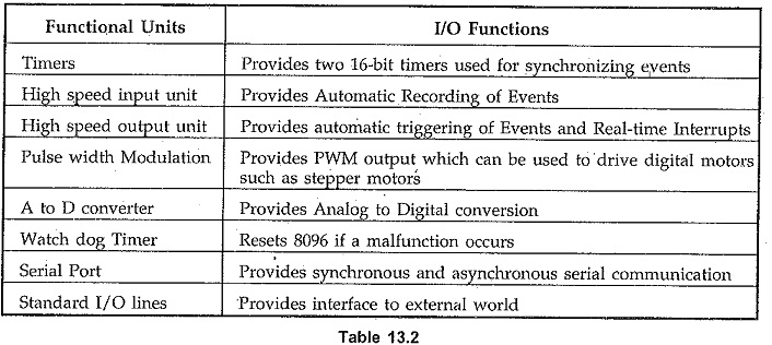
8096 Microprocessor Functional Units:
Table 13.2 shows the list of major I/O functions provided by various 8096 Microprocessor Functional Units.
Timers:
The 8096 Microprocessor Functional Units has two 16 bit timers. The first is designated as “Timer 1” and, the second, as “Timer 2”. Timer 1 is used to synchronize events to real time, while Timer 2 can be clocked externally and synchronizes events to external occurrences. The High Speed I/O unit is coupled to the timers in that the HSI records the value on Timer 1 when transitions occur and the HSO causes transitions to occur based on values of either Timer 1 or Timer 2.
Timer 1:
Timer 1 is clocked once every eight state times and can be cleared only by executing a reset. The only other way to change its value is by writing to 000CH but this is a test mode which sets both timers to OFFFXH and should not be used in programs.
Timer 2:
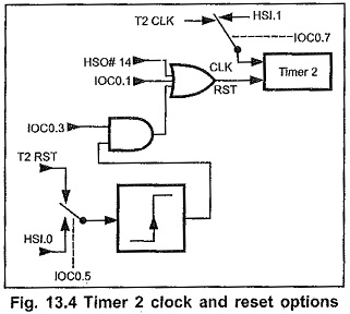
Timer 2 can be incremented by transitions (one count each transition, rising and falling ) on either T2CLK or HSI. 1. The multiple functionality of the timer is determined by the state of bit 7 in the I/O Control Register 0, (IOC0.7). Every count in the Timer 2 is compared with the contents of all registers in the content addressable memory (CAM). When match occurs interrupt is generated. In one state time, the count in the Timer 2 is compared with the contents of only one register in the CAM. There are 8 registers in the CAM. Therefore, the maximum transition speed for Timer 2 is limited to once per eight state times. Timer 2 can be cleared by following ways:
- Executing a reset,
- Setting IOC0. 1,
- Triggering HSO channel 0EH
- Pulling T2RST or HSI. 0 high.
Fig. 13.4 shows the different ways of manipulating Timer 2.
Timer Interrupts:
Both Timer 1 and Timer 2 can be used to trigger a timer overflow interrrupt and set a flag in the I/O status Register 1 (IOS1). The interrupts are controlled by IOC1.2 and IOC1.3 respectively. The flags are set in 1OS1.5 and 1O31.4 respectively. The general enabling and disabling of the timer interrupts are controlled by the Interrupt Mask Register bit 0. In all cases, setting a bit enables a function, while clearing a bit disables it.
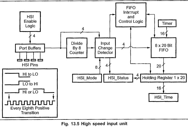
High Speed Inputs:
The High Speed Input Unit (HSI), can be used to record the time at which an event occurs with respect to Timer 1. There are 4 lines (HSI.0 through HSI.3) which can be used in this mode and up to a total of 8 events can be recorded HSI.2 and HSI.3 are bidirectional pins which can also be used as HSO.4 and HSO.5. The I/O Control Registers (IOC0 and IOC1) are used to determine the 8096 Microprocessor Functional Units of these pins. Fig. 13.5 shows the block diagram of the HSI unit.
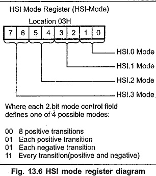
HSI Modes:
There are 4 possible modes of operation for each of the HSI. The HSI mode register is used to control which pins will look for what type of events. The 8-bit register is set up as shown in Fig. 13.6.
High and low levels of inputs need to be held for at least 1 state time to ensure proper operation. The maximum input speed is 1 event every 8 state times except when the 8 transition mode is used, in which one transition per state time is allowed.
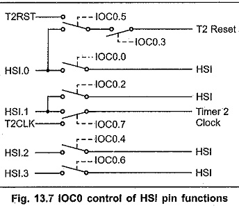
The HSI lines can be individually enabled and disabled using bits in IOC0, at location 0015H. Fig. 13.7 shows the bit locations which control the HSI pins.. If the pin is disabled, transitions will not be entered in the FIFO.
HSI FIFO:
When an HSI event occurs, a 8 x 20 FIFO stores the 16 bits of Timer 1 and the 4 bits indicating the state of the 4 HSI lines at the time the status is read. It can take up to 8 state times for this information to reach the holding register. For this reason, ,8 state times must be allowed between consecutive reads of HSITIME. When the FIFO is full, one additional event for a total of 8 events can be stored by considering the holding register as a part of the FIFO. If the FIFO and holding register are full any additional events will not be recorded and it will cause an overflow condition.
HSI Interrupts:
HSI Unit generates interrupts in one of the two ways, determined by 1OC1.7. If the bit is a 0, then an interrupt will be generated every time a value is loaded into the holding register. If it is. a 1, an interrupt will only be generated when the FIFO, (independent of the holding register) has six entries in it. Since all interrupts are rising edge triggered, if IOC1. 7 = 1, the processor will not be re-interrupted until the FIFO first contains 5 or less records, then contains six or more. Interrupts can also be generated by pin HSI.0, which has its own interrupt vector, location 2008H. Thus in all HSI unit generates interrupts by three ways.
HSI Status:
The status of the HSI FIFO is indicated by bits 6 and 7 of the I/O Status register 1 (1OS1). If bit 6 is a 1, the FIFO contains at least six entries. If bit 7 is a 1, the FIFO contains at least 1 entry and the holding register. has been loaded. The FIFO may be read after verifying that it contains valid data. While reading or testing bits in IOS1 it is necessary to store the byte and then test the stored value. Because reading or testing bits in IOS1,clears the entire byte, including the software and hardware timer overflow flags.
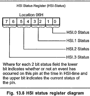
The HSI can be read is two steps. First, the HSI Status register is read to obtain the current state of the HSI pins and which pins had changed at the recorded time. Fig. 13.8 shows the format of the HSI_STATUS Register. Second, the HSI is read. Reading the Time register unloads one word of the FIFO, so if the Time register is read before the Status register, the information in the Status register will be lost. The HSI Status register is at location 06H and the HSI Time registers are in locations 04H and 05H.
If the HSI_TIME and Status register are read without the holding register being loaded, the values read will be undeterminable.
High Speed Outputs:
The High Speed Output unit (HSO) is used to trigger events at specific times with minimal CPU overhead. These events include : starting an A to D conversion, resetting Timer 2, setting 4 software flags, and switching up to 6 output lines. Interrupts can be generated whenever one of these events are triggered. Up to 8 events can be pending at any one time.
HSIO shared pins:
Two of the 6 output lines (HSO.0 though HSO.5) are shared with the High Speed Input (HSI) lines. HSO.4. and HSO.5 are shared with HSI.2 and HSI.3. respectively. Bits 4 and 6 of the I/O Control Register 1 (IOC1) are used to enable HSO.4 and HSO.5 as outputs.
HSO CAM:
Fig. 13.9 shows block diagram of the HSO unit. The Content Addressable Memory (CAM) file is the center of control. One CAM register is compared with a time value every state time. Therefore, it takes 8 state times to compare all CAM registers with a timer.
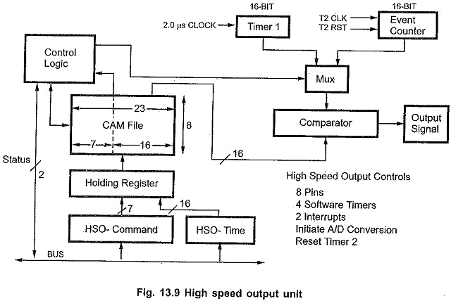
Each , CAM register is 23 bits wide. Sixteen bits specify the time at which the action is to be carried out and 7 bits specify both the nature of the action and whether Timer 1 or Timer 2 is the reference. The format of the command to the HSO unit is shown in the Fig. 13.10.
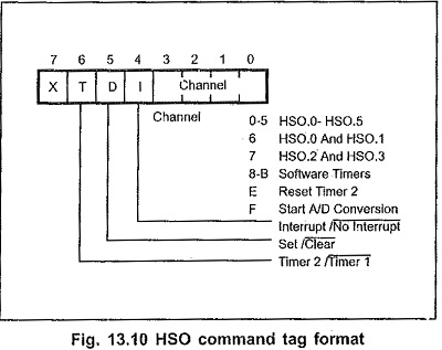
To enter a command into the CAM file, write the 7-bit “Command Tag” into location 0006H followed by the time at which the action is to be carried out into word address 0004H.
It is necessary to disable interrupts when writing the command tag for the HSO. If an interrupt occurs during the time between writing the command tag and loading the time value, and the interrupt service routine writes to the HSO time register, the command tag used in the interrupt routine will be written to the CAM. The command tag from the main program will not be executed.
HSO Interrupts:
The HSO unit can generate two types of interrupts : The HSO execution interrupt and the software timer interrupt. The HSO execution interrupt (vector = 2006H) is generated when HSO commands operate one or more of the six output pins. However, this interrupt is a maskable interrupt. The software timer interrupt is generated by any other HSO command such as triggering the A/D, resetting Timer 2 or generating a software time delay.
HSO Status:
Before writing to the HSO, Holding Register should be empty. If it is not, writing to the HSO will overwrite the value in the Holding Register. I/O Status Register (IOS0) bits 6 and 7 indicate the status of the HSO unit. If 10S0.6 equals 0, the holding register is empty and at least one CAM register is empty. If IOS0.7 equals 0, the holding register is empty.
Clearing the HSO:
All 8 CAM locations of the HSO are compared before any action is taken. This allows a pending external event to be cancelled by simply writing the opposite event to the CAM. However, once an entry is placed in the CAM, it cannot be removed until either the specified timer matches the written values or the chip is reset. Internal events are not synchronized to Timer 1, and therefore cannot be cleared. This includes events on HSO channels 8 through F and all interrupts. Since interrupts are not synchronized it is possbile to have multiple interrupts at the same time value.
Using Timer 2 with the HSO:
Timer 1 is incremented only once every 8 state-times. When it is being used as the reference timer for the HSO action, the comparator has a chance to look at all 8 CAM registers before Timer 1. changes its value. Following the same reasoning, Tinier 2 has been synchronized to allow it to change at a maximum rate of once per 8 state-times. Timer 2 increments on both edges of the input signal.
When using Timer 2 as HSO reference, caution must be taken that Timer 2 is not reset prior to the highest value for a Timer 2 match in the CAM. This is because the HSO CAM will hold an event pending until a time match occurs, if that match is to a time value on Timer 2 which is never reached, the event will remain pending in the CAM until the device is reset.
Additional caution must be used when Timer 2 is being reset using the. HSO unit. Since resetting Timer 2 using the HSO is an internal event and can therefore happen at any time within the eight-state-time window. For this reason, any events scheduled to occur at the same time as a Timer 2 reset should be logged into the CAM with a Timer 2 value of zero. When using this method to make a programmable modulo counter, the count will stay at the maximum Timer 2 value only until the Reset T2 command is recognized. The count will stay at zero for the transition which would have changed the count from “N” to zero, and then change to a one on the next transition.
Software Timers:
The HSO can be programmed to generate interrupts at preset times. Up to four such “Software Timers” can be in operation at a time. As each preprogrammed time is reached, the HSO unit sets a Software Timer Flag. If the interrupt bit in the command tag was set then a Software Timer Interrupt will also be generated. The interrupt service routine can then examine I/O Status register 1 (IOS1) to determine which software timer expired and caused the interrupt. When the HSO resets Timer 2 or starts an A to D conversion , it can also be programmed to generate a software timer interrupt but there is no flag to indicate that this has occurred. If more than one software timer interrupt occurs in the same time frame it is possible that multiple software timer interrupts will be generated.
Analog Inputs:
The A to D converter on the 8096 Microprocessor Functional Units provides 8-input channels with a 10-bit digital output. The channels are multiplexed. Successive approximation technique is used for conversion. The digital output is equivalent to the ratio of the input voltage divided by the analog supply voltage. If the. ratio is 1, then the result will be all ones. The A/D converter is available on the 8096, 8397, 8095 and 8395 members of the MCS-96 family. The A/D converter on the 8096 BH is slightly different than that on the 8096.
A/D Conversion Time and Formula:
8096
Each conversion requires 168 state-times (42 microseconds of the accuracy desired or value of input voltage.
8096 BH
Each conversion on 8096 Microprocessor Functional Units requires 88 state times (22 μsec at 12 MHz) independent of the accuracy desired or value of input voltage.
The analog input voltage should be in the range of 0 to VREF. The A/D result is calculated from the formula :
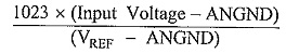
It can be seen from this formula that changes in VREF or ANGND effect the output of the converter. This can be advantageous if a ratiometric sensor is used since these sensors have an output that can be measured as a proportion of VREF.
A/D Commands:
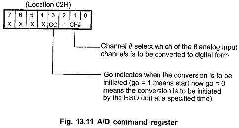
ACH0 through ACH7 are the 8 analog inputs, which are shared with port 0 pins. As we know channels are multiplexed any one of the 8 analog input pins is sampled for A/D conversion at a time. The A/D Command Register, at location 02H, selects which channel is to be converted and whether the conversion should start immediately or when the HSO (channel # 0FH) triggers it. The A/D command register must be written for each conversion, even if the HSO is used as the trigger. A to D commands are formatted as shown in, the Fig. 13.11.
A/D Output:
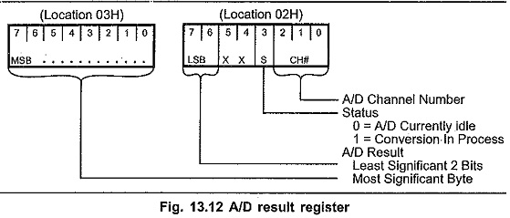
The output of the analog conversions are read from the A/D Result Register at locations 02H and 03H. Although these addresses are on a word boundary, they must be read as individual bytes. Fig. 13.12 shows the Information in the A/D Result register.
Pulse Width Modulation Output:
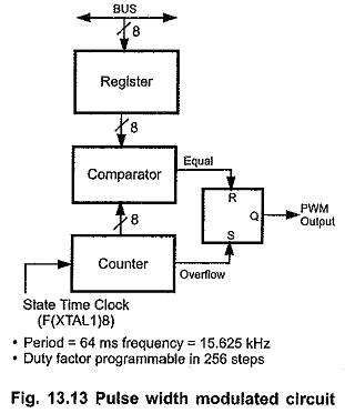
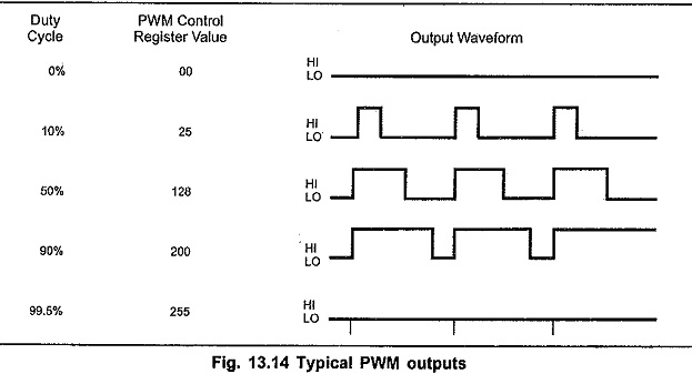
Fig. 13.13 shows the block diagram for pulse width modulation circuit. The main components of this circuit are PWM register, PWM counter and comparator. PWM output is set to one when counter value is 0. The 8-bit counter is incremented every state time. When the counter matches the value in the PWM register, the output is switched low. When the counter overflows, the output is once again switched high. A typical output waveform is shown in Fig. 13.14. It is important to note that when the PWM register equals 00, the output is always low.
Serial Port:
The serial port is compatible with the MCS-51 serial port. It has 3 asynchronous and one synchronous mode. The asyncronous modes are full duplex, meaning it can transmit and receive simultaneously. It is also double-buffered, meaning it can commence reception of a second byte before the previously received byte has been read from the receive register. The serial port registers for transmission (SBUF_Tx) and reception (SBUF_Rx) share the same address, 07H, but they are physically separate. (SBUF_Rx) contains data received by the serial port and (SBUF_Tx) hold data ready for transmission. The program cannot write to (SBUF_Rx) and read from (SBUF_Tx).
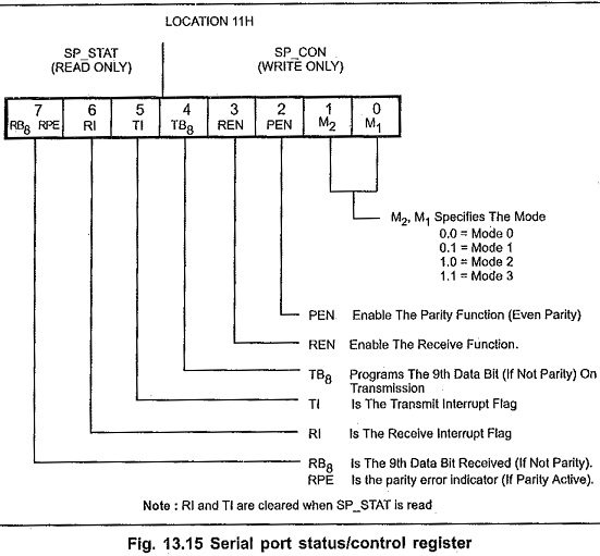
The format for Serial Port Status/Control register is shown in Fig. 13.15. The Serial Port Status/Control register at location 11H, is used to select the mode.