Interfacing of 8257 with 8085:
Fig. 14.68 shows the interfacing of 8257 with 8085 in I/O mapped I/O technique. In slave mode, RD and WR signals are activated by CPU when IO/M signal is high, indicating I/O bus cycle. In master mode DMA controller: (8257) generates MEMR,MEMW, IOR and IOW signals to control the data transfer between memory and I/O device.
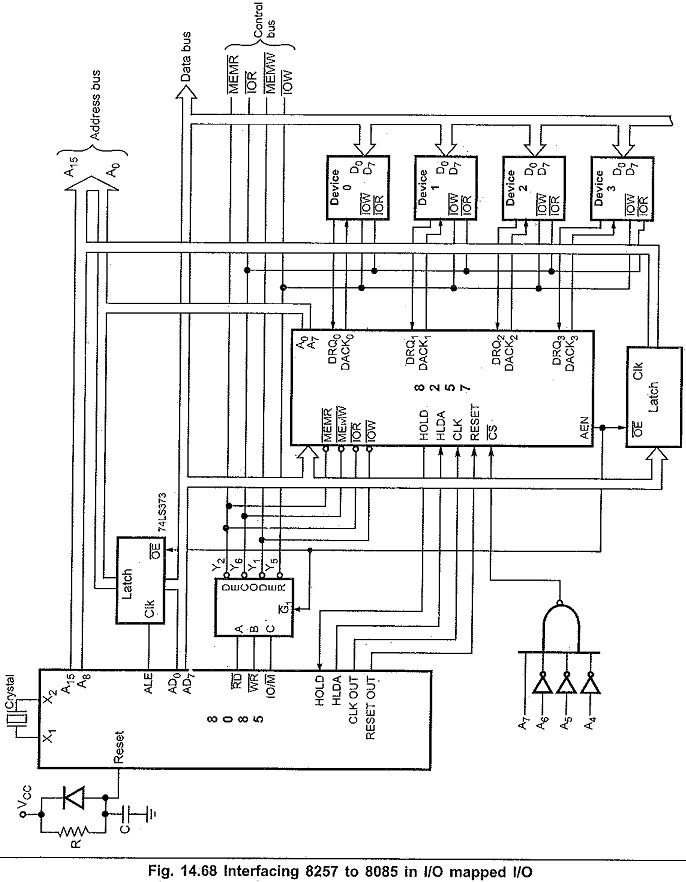
The function of the various components in the circuit are as follows :
- The 74LS373(1) latch is used to demultiplexed lower byte address and data bus.
- The 74LS138 (3:8 decoder) is used to generate MEMR, MEMW, IOR and IOW signals from RD, WR and IO/M signals.
- Another 74LS373(2) latch is used to demultiplexes higher byte address and data bus when DMA is master.
- AEN signal from 8257 is connected to the G1 signal of the 3:8 decoder and OE signal of latch. These connections make it possible to isolate system buses when DMA is in master mode.
- HOLD signal from Interfacing of 8257 with 8085 is connected to the HOLD input of 8085 and HLDA output of 8085 is connected to HLDA input of 8257. CLKOUT signal from 8085 is used to drive CLK input of 8257 and RESETOUT signal is used to drive RESET input of 8257.
Interfacing 8257 in Memory Mapped I/O:
The 8257 can be connected to the system bus as a memory device instead of as an I/O device. The interface is similar to I/O mapped I/O except the changes, in the connections as shown in the Fig. 14.69.
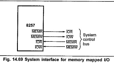
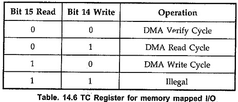
Here, the system memory control lines are connected to the I/O control lines of 8257 and system I/O control lines are connected to the memory control lines of 8257. Note that with these connections, the programming of the Read (bit 15) and write (bit 14) bits in the terminal count register will have a different meaning as shown in table.
Note : To get absolute address in memory mapped I/O, all remaining address lines (A15— A4) must be used to generate CS for the 8257.
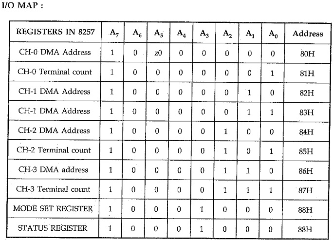
Programming 8257:
Programming of 8257 includes the loading of DMA address, terminal count and DMA transfer mode in the respective channel registers and mode set register. These registers are accessed by the CPU with unique addresses. Table 14.7 gives the internal logic used by the 8257 for the selection of registers.
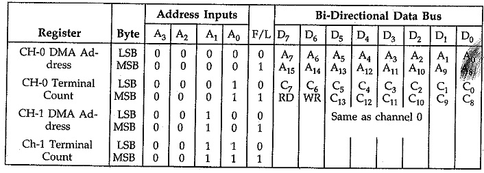
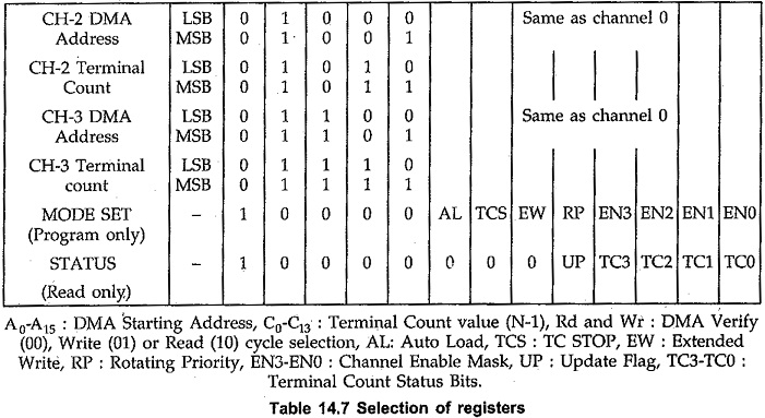
The least significant three address bits, A0 – A3, indicate the specific register to be accessed. As we know, channel registers are 16-bits two program instruction cycles are required to load or read an entire register contents. The Interfacing of 8257 with 8085 has flip flop which determines whether the upper or lower byte of the register is to be accessed. To maintain proper synchronization when accessing the “channel registers” all channel command instruction operations should occur in pairs, with the lower byte of a register always being accessed first.