IC Linear Voltage Regulators:
723 IC Regulator – The basic circuit of a 723 IC Linear Voltage Regulators in a dual-in-line package is shown in Fig. 17-20. This IC has a voltage reference source (D1), an error amplifier (A1), a series pass transistor (Q1), and a current limiting transistor (Q2), all contained in one small package. An additional Zener diode (D2) is included for voltage dropping in some applications. The IC can be connected to function as a positive or negative voltage regulator with an output voltage ranging from 2 V to 37 V, and output current levels up to 150 mA. The maximum supply voltage is 40 V, and the line and load regulations are each specified as 0.01%.
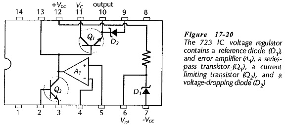
Figure 17-21 shows a 723 connected to function as a positive voltage regulator. The complete arrangement (including the internal circuitry shown in Fig. 17-20) is similar to the op-amp regulator circuit. One difference between the two circuits is the 100 pF capacitor (C1) connected to the error amplifier output and its inverting input terminal. This capacitor is used instead of a large capacitor at the output terminals to prevent the regulator from oscillating. (Sometimes both capacitors are required.) By appropriate selection of resistors R1 and R2 in Fig. 17-21, the regulator output can be set to any level between 7.15 V (the reference voltage) and 37 V. A potentiometer can be included between R1 and R2 to make the output voltage adjustable.
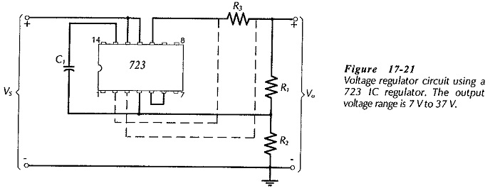
The dashed lines (in Fig. 17-21) show connections for simple (non-foldback) current limiting. Fold-back current limiting can also be used with the 723.
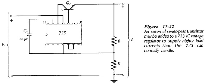
It is important to note that, as for all IC Linear Voltage Regulators circuits, the supply voltage at the lowest point on the ripple waveform should be at least 3 V greater than the regulator output; otherwise a high-amplitude output ripple might occur. The total power dissipation in the regulator should be calculated to ensure that it does not exceed the specified maximum. The specification lists 1.25 W as the maximum power dissipation at a free air temperature of 25°C for a DIL package. This must be derated at 10 mW/°C for higher temperatures. For a metal can package, PD(max) = 1 W at 25°C free air temperature, and the derating factor is 6.6 mW/°C. An external series-pass transistor may be Darlington-connected to (internal transistor) Q1, to enable a 723 regulator to handle larger load current. This is illustrated in Fig. 17-22.
A regulator output voltage less than the 7.15 V reference level can be obtained by using a voltage divider across the reference source (terminals 6 and 7 in Fig. 17-20). Terminal 5 is connected to the reduced reference voltage, instead of to terminal 6.
LM317 and LM337 IC Regulators:
The LM317 and LM337 IC Linear Voltage Regulators are three-terminal devices which are extremely easy to use. The 317 is a positive voltage regulator [Fig. 17-24(a)], and the 337 is a negative voltage regulator [Fig. 17-24(b)]. In each case, input and output terminals are provided for supply and regulated output voltage, and an adjustment terminal (ADJ) is included for output voltage selection. The output voltage range is 1.2 V to 37 V, and the maximum load current ranges from 300 mA to 2 A, depending on the device package type. Typical line and load regulations are specified as 0.01%/(volt of Vo), and 0 3%/(volt of Vo), respectively.
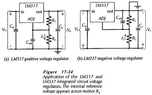
The internal reference voltage for the 317 and 337 regulators is typically 1.25 V, and Vref appears across the ADJ and output terminals. Consequently, the regulator output voltage is,
To determine suitable values for R1 and R2 for a desired output voltage, first select the voltage divider current (I1) to be much larger than the current that flows in the ADJ terminal of the device. This is specified as 100 μA maximum on the device data sheet. The resistors are calculated using the relationship in Eq. 17-7.
Note the capacitors included in the IC Linear Voltage Regulators circuits. Capacitor Cin is necessary only when the regulator is not located close to the power supply filter circuit. Cin eliminates the oscillatory tendencies that can occur with long connecting leads between the filter and regulator. Capacitor Co improves the transient response of the regulator and ensures ac stability, and Cadj improves the ripple rejection ratio.
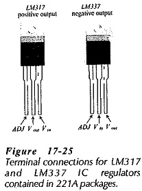
Figure 17-25 shows the terminal connections for LM317 and LM337 regulators in 221A-type packages.
LM340 Regulators:
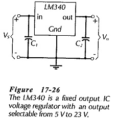
LM340 devices are three-terminal positive voltage regulators with fixed output voltages ranging from a low of 5 V to a high of 23 V. The regulator is selected for the desired output voltage and then simply provided with a voltage (VS) from a power supply filter circuit, as illustrated in Fig. 17-26. Here again, capacitor C1 is required only when the regulator is not located close to the filter.
The LM340 data sheet specifies the regulator performance for an output current of 1 A. The tolerance on the output voltage is ±2%, the line regulation is 0.01% per output volt, and the load regulation is 0.3% per amp of load current. The IC includes current limiting, and a thermal shutdown circuit that protects against excessive internal power dissipation. As with all series regulators, a heat sink must be used when high power dissipation is involved.