Transition and Diffusion Capacitance:
Transition and Diffusion Capacitance – Electronic devices are inherently sensitive to very high frequencies. Most shunt capacitive effects that can be ignored at lower frequencies due to very high reactance (XC being equal to 1/2πfC) cannot be ignored at very high frequencies. XC will become sufficiently small due to high value of frequency f to introduce a low reactance shorting path. In a P-N semiconductor diode, there are two capacitive effects to be considered. Both types of capacitances are present in the forward-bias and reverse-bias regions, but one so outweighs the other in each region that we consider the effects of only one in each region. In the reverse-bias region we have the transition or depletion-region capacitance (CT), while in the forward bias region we have the diffusion (CD) or storage capacitance.
Transition (or Space-Charge) Capacitance:
When a P-N junction is reverse biased, the depletion region acts like an insulator or dielectric material while the P- and N-type regions on either side have a low resistance and act as the plates. Thus P-N junction may be considered a parallel plate capacitor. The junction capacitance is termed as space-charge capacitance or transition capacitance or depletion region capacitance and is denoted by CT.
As mentioned earlier, a reverse bias causes majority carriers to move away from the junction, thereby uncovering more immobile charges. So the thickness W of the depletion layer increases with the increase in reverse bias voltage. This increase in uncovered charge with applied voltage may be considered a capacitive effect. The incremental capacitance CT may be defined as
![]()
where dQ is the increase in charge due to increase in voltage, dV.
![]()
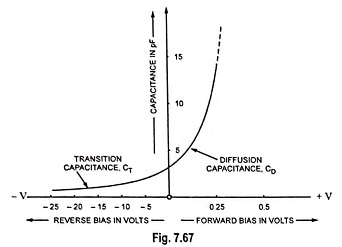
Since the depletion region increases with the increase in reverse-bias potential, the resulting transition capacitance decreases as shown in Fig. 7.67.
The fact that the capacitance depends on the applied reverse bias, has application in a number of electronic systems.
1. Step Graded Junction. A junction is said to be step graded if there is an abrupt change from acceptor ion concentration on the P-side to donor ion concentration on the N-side. Such a junction gets formed in alloyed junction or fused junction diode. Usually the acceptor density NA and the donor density ND are kept unequal.
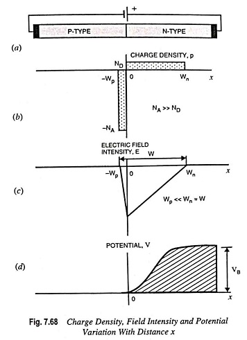
Figure 7.68 shows the charge density as a function of distance from an alloy junction in which acceptor impurity density is assumed to be much larger than the donor concentration. Since the net charge is zero,
![]()
When NA is much larger than ND, the Wp ≪ Wn and Wn ≈ W.
The relationship between potential and charge density is given by the Poisson’s equation,
![]()
where ∈ is the permittivity of the semiconductor and is given as ∈ = ∈r∈0 where ∈r is the relative permittivity of the dielectric and ∈0 is the permittivity of free space.
The electric lines of flux start on the positive donor ions and terminate on the negative acceptor ions. So there are no flux lines to the right of the boundary x = Wn in Fig. 7.68
and field intensity
![]()
at
![]()
Integrating Eq. (7.44) subject to these boundary conditions, we have
![]()
Neglecting the small voltage drop across Wp, we may arbitrarily choose V = 0 at x = 0
Integrating Eq. (7.45) subject to these conditions
![]()
The linear variation in field intensity and the quadratic dependence of potential upon distance are plotted in Fig. 7.68 (c) and (d).
At x = W, V = VB, the barrier height. Thus
![]()
Here VB = V0 – V where V is the negative number for an applied reverse bias and V0 is the contact potential.
Hence, the width of depletion layer increases with applied reverse bias and varies as √VB.
The total charge density of N-type material with area of junction A is given by
![]()
The transition capacitance CT, given by Eq. (7.41), is
![]()
From Eq. (7.47),
![]()
and therefore,
![]()
where ∈ is the absolute permittivity of the semiconductor medium, A is the cross-sectional area of the junction and W is the width of the depletion layer and is given as
![]()
Thus in a step graded junction, CT is inversely proportional to the square root of the junction voltage VB where VB is given as
![]()
where VR is a negative number indicating the applied reverse bias and V0 is the contact potential.
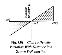
Linearly Graded Junction (or Grown Junction). A junction is said to he linearly graded if the charge density varies gradually (almost nearly) with the distance in the transition region. Such a junction gets formed in a growth junction diode.
In such a junction diode also, CT is given by Eq. (7.48). Thus the expression for CT for a linearly graded junction is the same as for a step graded junction. But here W is the total width of the space-charge layer. However, it now comes out that W varies as V1/3B instead of V1/2B.
Diffusion (or Storage) Capacitance:
When a P-N junction is forward biased, a capacitance, which is much larger than the transition capacitance, comes into play. This type of capacitance is called the diffusion capacitance, CD. We know that for a forward-biased P-N junction, the potential barrier is reduced. Now the electrons from N-side enter the P-side and holes from P-side enter into the N-side. These charge carriers diffuse away from the junction and progressively recombine. The density of charge carriers is high near the junction and decays exponentially with distance. Thus a charge is stored on both sides of the junction when forward biased. It is observed that the amount of stored charge varies with the applied potential as for a true capacitor. It is convenient to introduce an incremental capacitance, called diffusion or storage capacitance CD given by the equation CD = dQ/dV where dQ represents the change in number of minority carriers stored outside the depletion region when a change in voltage across diode, dV, is applied.
If τ is the mean lifetime of charge carriers, then a flow of charge Q yields a diode current I given as
![]()
and from Eq. (7.20),
![]()
So
![]()
So diffusion capacitance
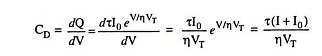
For a forward bias greater than a few tenths of a volt,
![]()
and according to Eq. (7.20) I ≫ I0 and so the diffusion capacitance is given as
![]()
Thus the diffusion capacitance is directly proportional to the forward current through the diode. This relationship occurs since the number of majority carriers injected into the depletion region is directly proportional to the forward current of the diode. The variation in diffusion capacitance with the variation in forward bias applied across a P-N junction is shown in Fig. 7.67.
This capacitance assumes great significance in the operation of devices which are required to switch rapidly from forward bias to reverse bias. Large value of CD, delays both of the switching-on and the switching-off.
In fact in a forward-biased diode, both the diffusion capacitance CD and the transition capacitance CT are present, but CD ≫ CT. Typically CD is more than a million times greater than CT. So in a forward-biased diode CT may be neglected and only CD may be considered. Typical value of CD is 0.02μF.
Similarly in a reverse-biased diode both CD and CT are present but CT ≫ CD. Hence in a reverse-biased diode CD is neglected and only CT is considered.
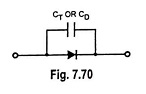
The capacitive effects described above may be represented by a capacitor connected in parallel with an ideal diode, as illustrated in Fig. 7.70.