Diffusion Process in IC Fabrication:
Diffusion is the oldest technique used to add impurity into the Substrate. The main aim of the Diffusion Process in IC Fabrication is to change the Conductivity of silicon substrate over a depth. The Diffusion Process in IC Fabrication is used in bipolar device technology to form bases, emitters, collectors ; while in MOS device technology to form source and drain region.
The impurity or dopant can be added into silicon by using one of the most commonly used methods given below,
- Diffusion from a chemical source at high temperatures,
- Diffusion from doped oxide source,
- Diffusion from an ion-implanted
The Diffusion Process in IC Fabrication is carried out at high temperature (about 900°C to 1250°C). The wafer placed in a chamber is exposed to the diffusant containing required impurity. In the chamber the wafer is placed in a quartz boat positioned in a quartz diffusion tube. The quartz tube holds a stack of vertically mounted wafers which all are diffused simultaneously. The equipment used for the oxidation process is used for the Diffusion Process in IC Fabrication. The diffusivities of the dopants in oxide and silicon decide the imperviousness of silicon dioxide to the diffusant.
The dopant may be in solid, liquid or gaseous form. The standard preferred p dopant is boron, while n dopants are antimony, arsenic, phosphorus. Arsenic is also preferred for n+ type source-drain and emitter diffusions. With dopants in solid state, the carrier gas, either nitrogen or oxygen, flows over a quartz boat containing dopant in powder form. With a liquid state dopant, the gas is bubbled over a liquid source in heated bath. With gaseous state dopant, there are problems of toxicity and chemical stability.
Diffusion Process in IC Fabrication takes place in one of the two modes,
- Single step mode, and
- Two step mode.
The first cycle is called predisposition diffusion. In this deposition the impurity concentration is maintained constant over the surface of the wafer. The impurity concentration at the surface of the substrate with a upper limit is called solid solubility. The solid solubility is a function of impurity and temperature. The second cycle in two step mode is called drive–in diffusion. In this cycle, dopant is removed. In the substrate, the impurity charges are redistributed. Thus using drive-in diffusion, the impurity concentration of the surface is reduced or even removed out of the substrate surface. It is generally combined with a regrowth of oxide over wafer using steam or oxygen gas. Depending upon the required profile of the diffused layer, the drive-in process either forms predeposition or carried out with the wafer.
1. Models of Diffusion in Solids:
The study of diffusion is based on two major approaches;
- continuum theory of Fick’s simple diffusion equation and
- atomistic theory.
The main objective of the study of the diffusion is to develop the models from experimental data. The main usefulness of this study is to calculate the important electrical characteristics of the semiconductor devices.
The continuum theory describes the diffusion phenomenon from Fick’s differential equation with correct boundary conditions and diffusities of impurity atoms. To explain concentration dependent diffusivities and anamalous diffusions, various atomic diffusion models have been developed. Let us now consider different models of diffusion in solids.
Diffusion, the atomic movement, in the solid can be realised as an atomic movement of diffusant in the crystal lattice by vacancies or self-interstitials. The common atomic diffusion models in a solid as shown in the Fig. 1.13.
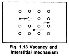
In the Fig. 1.13, the open circles represent the host atoms, while the solid circles represent either host impurity atoms. When the host atom gets sufficient energy during the vibration of lattice atoms, it tries to leave the lattice. Then such atom leaves the lattice creating a vacancy and itself becomes a self interstitial atom. The vacancy is indicated by a dotted circle. Now if the neighbouring atom, either host atom or impurity atom, moves to the vacancy created, then it is called diffusion by vacancy. If the atom moving to the vacancy is host atom, the diffusion is referred as self-diffusion. And if the atom moving towards the vacancy is an impurity atom, then the diffusion is called impurity diffusion. When the impurity atom migrates to a second vacancy that is at nearest distance from the original vacancy, then the diffusion is called diffusion by double vacancy or divacancy.
An atom smaller than host atom can not form covalent bonds with silicon. Such atom moves interstitially. ‘The movement of such interstitial atom from one place to other is called interstitial diffusion mechanism.
The interstitialcy mechanism is as shown in the Fig. 1.14.
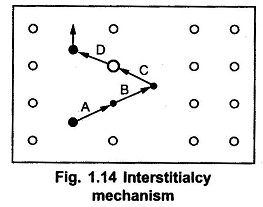
In a simple crystal lattice, the atomic movements of self interstitial atom displaces an impurity or dopant atom indicated by step A. Then in step B, the impurity atom becomes an interstitial atom. Such impurity atom displaces another host atom indicated by step C. The step D clearly indicates that, another host atom changes to self-interstitial atom. This mechanism is called extended interstitial mechanism or interstitialcy mechanism.
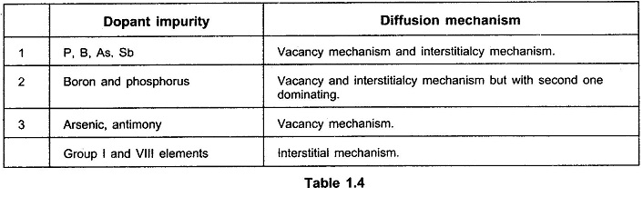
Following Table 1.4 indicates which mechanisms are dominant for different dopants.
2. Diffusion in SiO2:
To prevent diffusion of the impurity atoms into the silicon, the thermal oxide of silicon is most widely used as a mask in almost all the VLSI and silicon planar device fabrication.
In general, group III and group V elements form a glass in SiO2. Thus the melting temperature of the oxide film reduces. The diffusitives of the elements from group III and V depend on the concentration of the elements. A phosphorus forms a thin viscous film on SiO2. At 800°C to 900°C, the film flows. But outside the liquid solid boundary, because of low concentration, phosphorus can not show any diffusion.
The diffusivities of the dopant impurities, such as B, As, P and Sb, are very low, when their concentrations are very low. But some of the elements such as hydrogen, He, OH, Na, O2 and Ga are fast diffusants in SiO2 at around 900°C.
The diffusivity of As is a strong function of concentration. For low concentrations the diffusivities of As under diffusion in oxidizing condition and inert ambients are different. Under inert ambient conditions, As diffuses rapidly. In association with hydroxyl grough (OH or O2 / H2O), the diffusion enhances.
Upto 1200°C, Sb can not diffuse inside SiO2. But Sb diffuses at 900°C with N2 or O2 and O2 / H2O as ion implant.
Some metal elements such as Ag, Cu, Au, Pd and Ti, can diffuse in SiO2 under an electric field. This method is used in MOS structures to check reliability of the gate oxide. Au and Pd show no diffusion under applied field of ± 106 V/cm for 150 to 600°C temperature. While Ag diffuses with N2 at 300°C under electric field of 105 V / cm. Above 1100°C, under an applied electric field, sodium and potassium diffuses in SiO2 rapidly.
3. Diffusion Enhancements and Retardations:
Because of presence of defects and the high concentration effects, the diffusion study becomes complicated. Under the oxidizing ambient condition, the diffusion enhances or retards in silicon. The other process parameters also affect the lateral enhancement of diffusivity. All these conditions affect VLSI structures.
3.1 Effect of An Oxidizing Ambient:
When the diffusions of common impurity atoms (boron, phosphorus, arsenic and antimony) were tested in oxidising ambient under similar conditions. The oxidation enhanced diffusion of boron was first observed for <100> and <111> oriented silicon for high concentrations. Then the efforts were taken to study the diffusion separating the high concentration effects by introducing dopants at low concentrations. Thus ion implanted layer was formed. A thin layer of oxide was grown at low temperatures followed by relatively thick layer of silicon nitride. It was observed that the thin oxide layer is useful in adjusting the interface properties. Without this layer, surface leakage currents caused instabilities. Then using photolithography and etching techniques strips of silicon nitride and silicon were removed. Then it was observed that under oxidising ambient conditions, these samples oxidised at different oxidation temperatures for different time periods for <100> and <111> oriented silicon wafers.
The enhancement and retardation in diffusion can be calculated by measuring the junction depths from the original sample surface prior to oxidation, but before the deposition of silicon nitride layer. The diffusivity under oxide is given by
![]()
where
- Di = intrinsic diffusivity in non oxidizing ambient
- DA = diffusivity under oxidizing ambient
- Δ D = enhancement diffusivity
Similarly the enhancement and retardation depth Δ xj is given by
![]()
where
- Δ xj = enhancement or retardation depth
- (xj) f0 = final junction depth under oxide
- (xj) f = final junction depth under silicon oxide and nitride mask
The oxidation enhancement of As and P is studied using prediffused samples. Following are the results of the above mentioned investigations.
- In dry N2, for <100> and <111> oriented silicon wafers, diffusivities are same for As and P.
- In dry O2, for As and P, the diffusivities are enhanced in <100> oriented But in <111> oriented silicons, the diffusivity for P is enhanced, but for As only a little enhanment is observed.
- The enhancement is more in <100> oriented silicon as compared to <111> oriented silicon.
- For short oxidation time, the enhancement is greater and vice a versa.
The heat treatment of silicon dioxide film in N2 , NH3 or H2 + N2 is called direct nitridation. Under direct nitridation, the diffusion of the impurity is dominent by vacancy mechanism. The diffusivities of boron and phosphorus during oxidation depend on dual mechanism i.e. vacancy and interstitialcy mechanism.
3.2 Lateral Enhancement of Diffusivity:
In narrow oxide and silicon nitride layers, the diffusion process is enhanced due to the anomalous junction depths. In boron, under nitride layer, diffusion enhances. In narrow strips the diffusion enhances due to the enhanced and non-uniform junction depths.