Fabrication of Monolithic IC:
The cross-sectional view of an Fabrication of Monolithic IC and discrete planar transistor are as shown in the Fig. 1.17 (a) and (b) respectively.
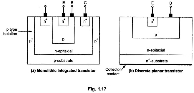
The main difference between Fabrication of Monolithic IC and discrete planar transistor is that collector contact in monolithic integrated transistor is at top, while in the discrete planar transistor it is at bottom.
Because of this the collector series resistance of the collector current path increases. This effectively increases the collector to emitter voltage VCE(sat) of the device.
Also in Monolithic integrated transistor as substrate is held at negative potential, additional parasitic capacitance appears between collector and substrate.
Buried Layer:
To overcome the increase in collector series resistance, buried n+ layer is encorporated by using additional process step. The buried layer can be processed with heavily doped n+ region in between p-type substrate and n-type epitaxial collector.
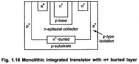
The advantage of burried n+ layer is that it provides low resistivity current path as shown in the Fig. 1.18. The buried n+ layer shunts n-epitaxial collector layer effectively decreasing resistance.