Op Amp Voltage Regulators:
Voltage Follower Regulator – Refer once again to the Op Amp Voltage Regulators circuit in Fig. 17-11. The complete error amplifier has two input terminals at the bases of Q5 and Q6 and one output at the collector of Q2, Transistor Q6 base is an inverting input and Q5 base is a noninverting input. The error amplifier circuit Is essentially an operational amplifier. Thus, IC operational amplifiers with their extremely high open-loop voltage gain are ideal for use as error amplifiers in dc voltage regulator circuits. Normally, an internally compensated op-amp (such as the 741) is quite suitable for most voltage regulator applications.
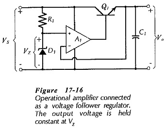
A simple voltage follower regulator circuit is illustrated in Fig. 17-16. In this circuit, the op-amp output voltage always follows the voltage at the noninverting terminal, consequently, Vo remains constant at VZ. The only design calculations are those required for design of the Zener diode voltage reference circuit (R1 and D1), and for the specification of Q1.
Adjustable Output Regulator:
The circuit in Fig. 17-17 is that of a variable-output, highly stable de voltage regulator. As shown already in transistor circuit, the reference diode in Fig. 17-17 is connected at the amplifier noninverting input, and the output voltage is divided and applied to the inverting input. The operational amplifier positive supply terminal has to be connected to regulator supply voltage. If it were connected to the regulator output, the op-amp output voltage (at Q2 base) would have to be approximately 0.7 V higher than its positive supply terminal, and this is impossible.
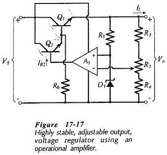
Design of the regulator circuit In Fig. 17-17 involves selection of R1 and D1, design of the voltage divider network (R3, R4, and R5), and specification of transistors Q1 and Q2. Clearly, an op-amp voltage regulator is more easily designed than a purely transistor regulator circuit.
Current Limiting with an Op-amp Regulator:
When a large output current is to be supplied by an operational amplifier voltage regulator, one of the current limiting circuits described already may be used with one important modification. Figure 17-19 shows the modification. A resistor (R13) must be connected between the op-amp output terminal and the Junction of Q2B and Q7C.
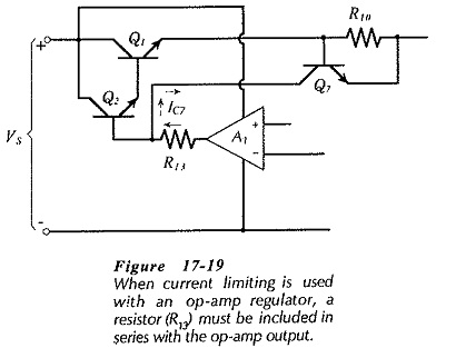
When an overload causes the regulator output voltage to go to zero, the op-amp output goes high (close to VS) as it attempts to return Vo to its normal level. Consequently, because the op-amp normally has a very low output resistance, R13 is necessary to allow IC7 to drop the voltage at Q2 base to near ground level. The additional resistor at the op-amp output is calculated as R13 ≈ VS/IC7. Resistor R13 must not be so large that an excessive voltage drop occurs across it when the regulator is supposed to be operating normally.