Transistor Voltage and Current:
The Transistor Voltage polarities for an npn transistor are shown in Fig. 4-10(a). As well as conventional current direction, the direction of the arrowhead indicates the transistor bias polarities. For an npn transistor, the base is biased positive with respect to the emitter, and the arrowhead points from the (positive) base to the (negative) emitter. The collector is then biased to a higher positive Transistor Voltage than the base.
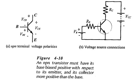
Figure 4-10(b) shows that the Transistor Voltage sources are usually connected to the transistor via resistors. The base bias voltage (VB) is connected via resistor RB, and the collector supply (VCC) is connected via RC. The negative terminals of the two voltage sources are connected at the transistor emitter terminal. VCC is always much larger than VB, and this ensures that the CB junction remains reverse biased; positive on the collector (n-side), and negative on the base (p-side).
Typical transistor base-emitter voltages are similar to diode forward voltages; 0.7 V for a silicon transistor, and 0.3 V for a germanium device. Typical collector voltages might be anything from 3 V to 20 V for most types of transistors, although in many the collector Transistor Voltage may be greater than 20 V.
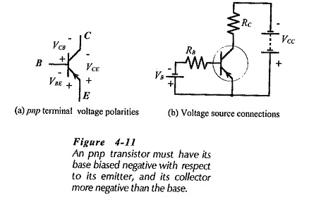
For a pnp device [Fig. 4-11(a)] the base is biased negative with respect to the emitter. The arrowhead points from the (positive) emitter to the (negative) base, and the collector is made more negative than the base. Figure 4-11(b) shows the Transistor Voltage sources connected via resistors, and the source positive terminals connected at the emitter. With VCC larger than VB, the (p-type) collector is more negative than the (n-type) base, keeping the CB junction reverse biased.
All transistors (npn and imp) are normally operated with the CB junction reverse biased and the BE junction forward biased. In the case of a switching transistor, (a transistor that is not operated as an amplifier, but is either switched on or off), the CB junction may become forward biased by approximately 0.5 V. Also, in transistor switching circuits (and some other circuits) the BE junction can become reverse biased.
Transistor Currents:
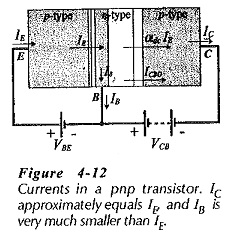
The various current components that flow within a transistor are illustrated in Fig. 4-12. The current flowing into the emitter terminal is referred to as the emitter current and is identified as IE. For the pnp device shown, IE can be thought of as a flow of holes from the emitter to the base. Note that the indicated IE direction is the conventional current direction from positive to negative. Base current IB and collector current IC are also shown as conventional current direction. Both IC and IB flow out of the transistor. while IE flows into the transistor, (see Fig. 4-12 and 4-13). Therefore,
![]()
As already discussed, almost all of IE crosses to the collector, and only a small portion flows out of the base terminal. Typically 96% to 99.5% of IE flows across the collector-base junction to become the collector current. As shown in Fig. 4-12,
![]()
αdc (alpha dc) is the emitter-to-collector current gain, or the ratio of collector current to emitter current. From Eq. 4-2, αdc = IC /IE. Numerically, αdc is typically 0.96 to 0.995. So, the collector current is almost equal to the emitter current, and in many circuit situations IC is assumed equal to IE. For reasons that will be explained later, αdc is termed the common-base dc current gain.
Because the CB junction is reverse biased, a very small reverse saturation current (ICBO) flows across the junction, (see Fig. 4-12). ICBO is named the collector-to-base leakage current, and it is normally so small that it can be neglected.
Substituting for IE from Eq. 4-1 into Eq. 4-2,
![]()
which gives,
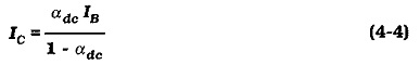
Equation 4-4 can be rewritten as,
![]()
Where,
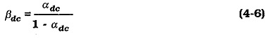
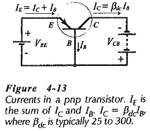
βdc (beta dc) is the base-to-collector current gain, or the ratio of collector current to base current, (see Fig. 4-13). From Eq. 4-5, βdc = IC /IB. Typically, βdc ranges from 25 to 300. As will be explained, βdc is also termed the common-emitter dc current gain. Instead of βdc another symbol for common-emitter dc current gain is hFE. This originates from the hFE parameter circuit discussed in Section 6-3. h is the symbol used on transistor data sheets.
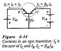
Although Equations 4-1 through 4-6 were derived for a pnp device, they apply equally to npn transistors. One difference in the case of an npn transistor is that IB and IC are assumed to flow into the device (conventional current direction), and IE is taken as flowing out, (see Fig, 4-14). As explained already, electrons are the majority charge carriers in an npn transistor, and they move in a direction opposite to conventional current direction
Typical collector and emitter currents for low-power transistors range from 1 mA to 25 mA, and base currents are usually less than 100 μA. High power transistors handle currents of several amps