Transformer Coupled Amplifier:
Transformer Coupled Amplifier commences with the load resistance and output power, specification. A signal voltage amplitude may also be stated, as well as the upper and lower cutoff frequencies for the amplifier. If a supply, voltage is given, then the design must determine a specification for the transformer. Where an available transformer is to be employed, the supply voltage is calculated to suit the transformer. The maximum levels of VCE,IC, and PD must be calculated for each transistor.
Transformer Coupled Amplifier Theory:
The power delivered to the transformer primary is determined by,
The power delivered to the primary can also be expressed as,
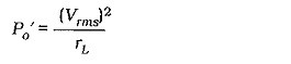
where Vrms is the rms primary voltage, and rL is the ac resistance offered by the transformer primary (the referred resistance). Using peak voltages, the equation becomes,
![]()
This gives the equation for rL:
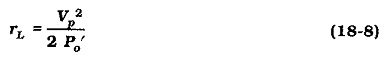
Using Eq. 18-2, rL can be calculated in terms of the load resistance and the transformer turn ratio:

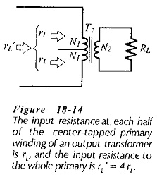
The resistance seen when “looking into” the whole winding of a transformer with a center tapped primary winding (see Fig. 18-14) is,
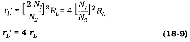
The transformer can now be specified in terms of the output power (Po), the load resistance (RL), and the referred resistance (rL‘).
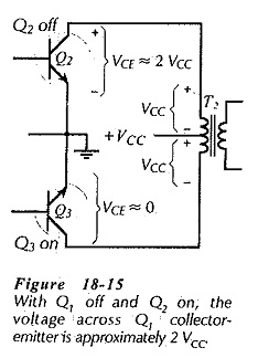
Referring to Fig. 18-15, note that when Q2 is off and Q3 is on a voltage with a peak value of approximately +VCC is induced in the half of the transformer primary connected to Q2. The induced voltage occurs because the other half of the primary has +VCC applied to it via Q3, and because both windings are on the same magnetic core. The induced voltage is superimposed upon the supply, so that the voltage that appears at the collector of Q2 is,
![]()
To determine the peak transistor current, the equation for power delivered to the transformer primary is rewritten. From Eq. 18-5,
![]()
The power dissipated in the two output transistors is the difference between the dc supply power to the Transformer and the ac power delivered to the transformer primary:
![]()
Each transistor is on for half of each cycle of the input signal, so the power dissipated in each transistor is half of 2 PT.
![]()
The transistors are specified in terms of the device power dissipation (PT), the peak current (Ip), and the maximum collector-emitter voltage (VCE(max)). The transistors must also be operated below the maximum power dissipation curve.
Advantages and Disadvantages of Transformer Coupled Amplifier:
Poor frequency response is one disadvantage of Transformer Coupled Amplifier Design, both at the low and high ends of the audio frequency range. This can be improved by the use of overall negative feedback. However, substantial improvement in frequency response can be achieved by eliminating transformers from the circuit. The alternatives are capacitor coupling and direct coupling of the amplifier load.