Transformer Coupled Class B Amplifier:
Class B Amplifier – The inefficiency of Class-A amplifiers is largely due to the transistor bias conditions. In a Class-B amplifier, the transistors are biased to cutoff, so that there is no transistor power dissipation when there is no input signal. This gives the Transformer Coupled Class B Amplifier a much greater efficiency than the Class-A circuit.
The output stage of a Class-B transformer-coupled amplifier is shown in Fig. 18-8. Transformer T2 couples load resistor RL, to the collector circuits of transistors Q2 and Q3. Note that the supply is connected to the center-tap of the transformer primary, and that Q2 and Q3 have grounded emitters. The transistor bases are grounded via resistors R1 and R2, so that both are biased off.
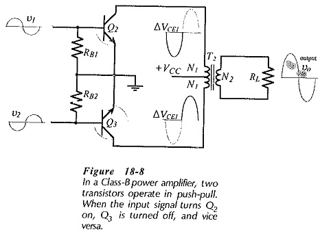
The input signals applied to the transistor bases consist of two separate sine waves which are identical, except that they are in antiphase. When v1 is going positive, v2 is going negative, so that Q3 is being biased further off as Q2 is being biased on. As the collector current in Q2 increases from zero, it produces a half sine wave of voltage across the upper half of the transformer primary, as illustrated. When the positive half-cycle of input signal to Q2 base begins to go negative, the signal at Q3 base is commencing to go positive. Thus, as Q2 becomes biased off again, Q3 is biased on, and a half-cycle of voltage waveform is generated across the lower half of the transformer primary.
The two half-cycles in the separate sections of the transformer primary produce a magnetic flux in the transformer core that flows first in one direction and then in the opposite direction. This flux links with the secondary winding and generates a complete sine wave output which is passed to the load.
In the Class-B circuit, the two output transistors are said to be operating in push-pull. The push-pull action is best illustrated by drawing the ac load line on the composite characteristics for Q2 and Q3. The composite characteristics are created by drawing the Q2 characteristics in the normal way, and presenting the Q3 characteristics upside down. This is illustrated in Fig. 18-9.
Now consider the effect of a signal applied to the bases of Q2 and Q3 in the circuit in Fig. 18-8. When IB1 is increased from zero to 90 μA, Q3 remains off and VCE1 falls to 1.6 V, (point C on the composite characteristics in Fig. 18-9). At this point the voltage across the upper half of the transformer primary in is,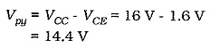
When IB2 is increased from 0 to 90 μA, Q2 is off, and the Q3 current and voltage conditions move to point D on the ac load line. This produces 14.4 V across the lower half of the transformer primary. Thus, a full sine wave is developed at the transformer output. When no signal is present, both transistors remain off and dissipate zero power. Power is dissipated only while each device is conducting. The wasted power is considerably less with the Class-B amplifier than with a Class-A circuit.
Crossover Distortion:
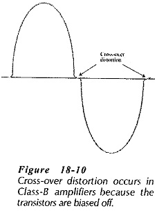
The waveform delivered to the transformer primary and the resultant output are not perfectly sinusoidal in the Class-B circuit. Cross-over distortion is produced in the output waveform, as illustrated in Fig. 18-9 and 18-10, due to the fact that the transistors do not begin to turn on until the input base-emitter voltage is about 0.5 V for a silicon device, or 0.15 V for a germanium transistor. To eliminate this effect, the transistors are partially biased on instead of being biased off With this modification, the Class-B amplifier becomes a Class-AB amplifier.
Class AB Amplifier:
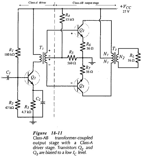
Figure 18-11 shows a Class-AB transformer-coupled output stage with a Class-A transformer-coupled driver stage. The output transformer (T2) has a center-tapped primary winding, with each half of the winding constituting a load for one of the output transistors (Q2 and Q3). Resistors R4 and R5 bias Q2 and Q3 partially on, and resistors R6 and R7 limit the emitter (and collector) currents to the desired bias levels. Transformer T1 together with transistor Q2 and the associated components comprise a Class-A stage. The secondary of T1 is center-tapped to provide the necessary antiphase signals to Q2 and Q3.
When the instantaneous polarity of T1 output is positive at the top, Q2 base voltage is positive and Q3 base voltage is negative, as illustrated. At this time Q2 is on and Q3 is off. When the polarity reverses at T1 output, the base of Q3 becomes positive and that of Q2 becomes negative. The output stage functions exactly as for a Class-B circuit, except that each device commences to conduct just before the signal to its base becomes positive. This eliminates the transistor turn-on delay that creates crossover distortion in a Class-B amplifier.
The Class-A portion of the circuit in Fig. 18-11 is referred to as a driver stage, simply because it provides the input signals to drive the Class-AB output stage. The input power handled by the driver stage is very much smaller than the circuit output power, so that the inefficiency of the Class-A stage is unimportant.
Efficiency of Class-B and Class-AB Amplifiers:
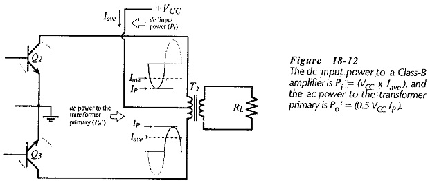
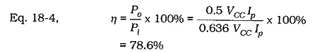
For a Class-B amplifier, the dc supply power (see Fig. 18-12) is calculated as,
The ac power input to the transformer primary is given by Eq.18-5,
![]()
Assuming a 100% efficiency for the output transformer,
![]()
So, the maximum theoretical efficiency for a Class-B transformer-coupled power amplifier is,
Once again, the efficiency of a practical amplifier is lower than the theoretical efficiency. Some power is wasted in the transistors and emitter resistors, and the transformer is never 100% efficient.
The efficiency of a Class-AB power amplifier is typically a little less than that of a Class-B circuit, because of the additional small amount of power wasted in keeping the output transistors biased in a low-current on state. Class-B and Class-AB power amplifiers are employed more often than Class-A circuits, because of their greater efficiency,