Light Emitting Materials:
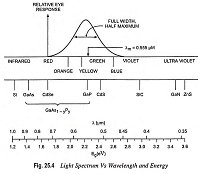
Since the eye is only sensitive to light of energy hf ≥ 1.8 eV (~ 0.7 μm), semiconductors of interest must have energy band gaps larger than this limit. The band gaps of different binary compound Light Emitting Materials semiconductors are illustrated in Fig. 25.4. A large variation exists in photon energy between the infrared band gaps (InSb of 0.18 eV) to the ultraviolet band gap (GaN of 3.4 eV).
In fact, use of ternary and quatenary compounds can increase number of available energy significantly. A good example, of the variation in photon energy available from the compound semiconductors is the ternary alloy gallium arsenide-phosphide, as illustrated in Fig. 25.62. With the decrease in percentage of As and increase in percentage of P, the resulting band gap varies from the indirect 1.43 eV gap of GaAs (infrared) to the indirect 2.26 eV gap of GaP (green). The band gap of GaAs1-xPx varies almost linearly with x until the 0.45 composition is reached, and electron-hole recombination is direct over this range. The most common alloy composition employed in LED displays is x ≈ 0.4. For this composition the band gap is direct. This results in efficient radiative recombination, and the emitted photons (~1.9 eV) are in the red portion of the spectrum.
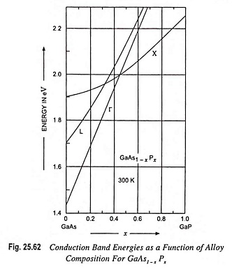
For GaAs1-xPx with P concentrations exceeding 45 percent, the band gap is due to the indirect X minimum. Radiative recombination in such indirect materials is generally unlikely, since electrons in the conduction band have different momentum from holes in the valence band.
However, indirect GaAs1-xPx (including GaP, x = 1) doped with nitrogen can be employed in LEDs to provide light in the yellow to green spectrum. This is possible because the nitrogen impurity binds an electron very tightly.
Application of Light Emitting Materials:
In many applications light from a laser or an LED need not be visible to the eye. Infrared emitters like InP, GaAs, and mixed alloys of such compounds are well suitable for optical communication systems. For instance, we can employ a laser or LED in conjunction with a photodiode or other photosensitive device for transmission of information optically between locations. By variation of current through the diode, the light output can be modulated such that analog or digital information appears in the optical signal directed at the detector. Alternatively the information may be introduced between the source and detector. For instance, a semiconductor laser-photodetector arrangement may be employed in a compact disc system for reading digital information from the spinning disc. Optoelectronic pair formed by a light emitter and a photodiode provides complete electrical isolation between input and output, because the only link between the two devices is optical.
A large number of available compound III-IV semiconductor materials have proved useful to provide for increased number of applications using semiconductor lasers and LEDs with visible and infrared wavelengths. In addition to the AIGaAs and GaAsP systems, the InAIGaP system is useful for yellow and green wavelengths and a GaN is a strong emitter in the blue. Even more wavelengths will be accessible as GaN and related materials are increasingly employed in LEDs and LASERS. With traditional doping methods, crystal defects tend to compensate the doping impurities such that N-type (ZnS, ZnSe, CdS, CdSe) or P-type (ZnTe) can be obtained. With the use of a nitrogen plasma source, ZnTe can be doped P-type to acceptor concentrations exceeding 1025/m-3. The availability of blue light from GaN is particularly important in extending III-V light emission across the entire visible spectrum.