DC Feedback Pair with Two Amplification Stages:
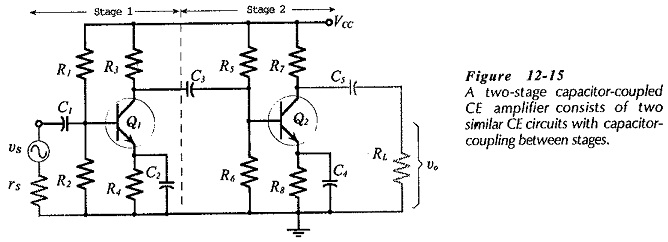
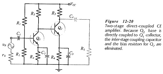
The DC Feedback Pair with Two Amplification Stages circuit shown in Fig. 12-25(a). The base of transistor Q2 is directly connected to the collector of Q1, and the base of Q1 is biased from the emitter of Q2 via resistor R2. Comparing this circuit to the capacitor-coupled circuit of Fig. 12-15 and the direct-coupled circuit of Fig. 12-20, it is seen that a further saving in components has been effected: R1, R2, R4, and C2 in Fig. 12-20 are now replaced with the single resistor R2 in Fig. 12-25.
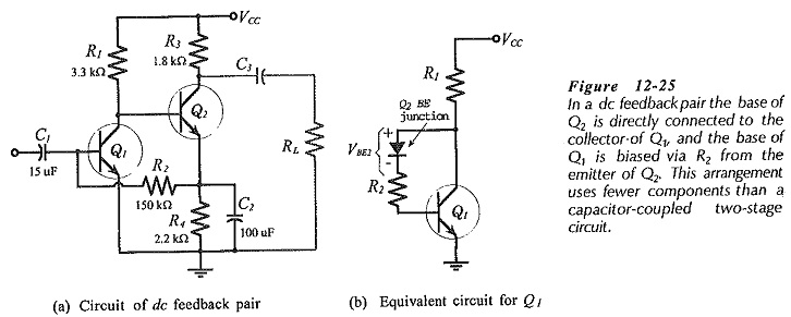
To understand the bias arrangement for the DC Feedback Pair with Two Amplification Stages, note that there is only a pn junction voltage drop VBE2 between the Q1 collector and the Q2 emitter. This is illustrated in Fig. 12-25(b), where it is seen that the first stage of the circuit is essentially a collector-to-base bias circuit. Stage 2 bias arrangement is similar to voltage divider bias, with resistor R4 stabilizing the transistor emitter current. The base voltage for Q2 is derived from the collector of Q1; consequently, the bias stability of the second stage is no better than that of the first stage.
Because collector-to-base bias is not as stable as voltage divider bias, the bias conditions in this circuit are not as stable as in the circuit of Fig. 12-20. However, the stability is adequate for most purposes, and the component savings can be a major advantage.
The DC Feedback Pair with Two Amplification Stages derives its name from the direct coupling between stages and from the feedback from the collector of Q1 to its base. As explained for collector-to-base bias already, a change in the level of Q1 collector voltage (VC1), produces a change in base current (IB1). The IB1 change in turn alters IC1, and the voltage drop IC1R1 tends to push VC1 back towards its original level.
As well as stabilizing the circuit dc conditions, the feedback can produce ac degeneration. Capacitor C2 shorts the ac feedback to ground, to eliminate ac degeneration from Stage 1. As the emitter bypass capacitor, C2 also eliminates ac degeneration from Stage 2.
The design approach to the DC Feedback Pair with Two Amplification Stages is similar to those already discussed. The output stage is designed exactly like the output stage for the direct-coupled circuit in Fig. 12-20. The input stage is designed as a collector-to-base bias circuit to have a collector voltage (VC1) equal to the desired level of the Stage 2 base voltage (VB2).
The input impedance of the circuit is
![]()
So, The impedance of C1 at f1 is,
C2 is by far the largest capacitor in the circuit, so it determines the circuit low 3 dB frequency:
C3 is once again calculated as,
DC Feedback pair with Emitter Follower Output:
Figure 12-26 shows a dc feedback pair that has an emitter follower output stage. In this case, a bypass capacitor cannot be used at the emitter of Q2, otherwise the output would be ac shorted to ground. However, C2 in Fig. 12-25 also serves the purpose of eliminating ac feedback from the collector of Q1 to its base (via Q2). So, now another method of removing this ac feedback must be employed. In Fig. 12-26, the base bias resistor for Q1 is split into two resistors, and the Junction of these two is ac grounded via capacitor C2.
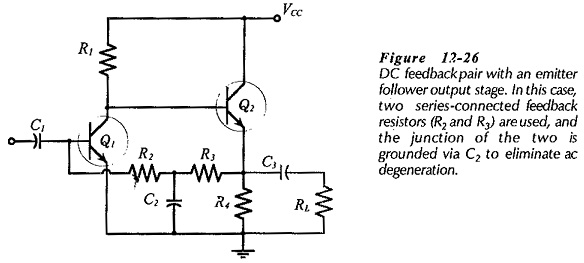
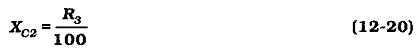
The design of this circuit differs from other designs only in calculation of the capacitor values. In this case, XC2 should be very much smaller than R3 at f1. This is because the ac output voltage at the emitter of Q2 is divided across R3 and XC2 before being fed back to the Q1 base. Capacitor values normally depend on the resistance in series with them, and in Fig. 12-26 R3 is in series with C2 for ac feedback. Because this capacitor is in the feedback path from output to input, it is calculated at f1 from
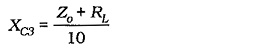
Normally, the largest capacitor in any circuit is employed to determine the circuit low 3 dB frequency (f1). Where two capacitors are likely to be equally large, they are both used to set f1. The largest capacitor is always the one in series with the lowest resistance. In the circuit in Fig. 12-26, the external load resistance is likely to be the smallest resistance in series with a capacitor. Consequently, C3 is calculated from,
![]()