Pulse Width Modulation(PWM):
Pulse width modulation of PTM is also often called Pulse Duration Modulation (PDM). In this system, shown in Fig. 18.8, we have a fixed amplitude and starting time of each pulse, but the width of each pulse is made proportional to the amplitude of the signal at that instant.
In Fig. 18.8, there may be a sequence of signal sample amplitudes of (say) 0.9, 0.5, 0 and — 0.4 V. These may be represented by pulse widths of 1.9, 1.5, 1.0 and 0.6 μs. In this system the width corresponding to zero amplitude can be selected as 1.0 μs, assuming that the signal amplitude varies at this point between + 1 V (width = 2 μs) and — 1 V (width = 0 μs). Zero amplitude is thus the averaging signal level, which corresponds to the average pulse width of 1 ,us
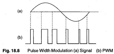
In this contrast, a negative pulse width is not possible, because it would make the pulse end before it began. If the pulse in a practical system has a recurrence rate of 8000 pulses/s the time of starting the adjoining pulses is 106/ 8000 = 125 μs. This is enough to not only accommodate varying widths but also to permit time division multiplexing (106 = 1 MHz frequency clock).
Generation and Demodulation of PWM:
Pulse width modulation may be generated by applying trigger pulses (at the sampling rate) to control the starting time of pulses from a monostable miltivibrator, and feeding in the signal to be sampled to control the duration of the pulses. The circuit diagram for such an arrangement is shown in Fig. 18.9.
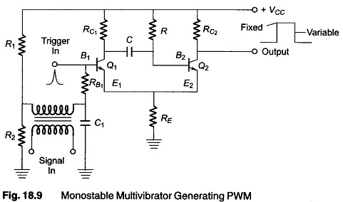
The emitter-coupled monostable multivibrator shown in Fig. 18.9 makes an excellent voltage to time converter, since its gate width is dependent on the voltage to which the capacitor C is charged. If this voltage is varied in accordance with a signal voltage, a series of rectangular pulses are obtained,with widths varying as required. The circuit performs two functions; it samples, and converts this sample in Pulse Width Modulation.
The operation of the circuit is as follows.
The multivibrator is in the stable state when Q1 — OFF and Q2 — ON. The applied trigger pulse switches Q1 — ON, and thereby the voltage at C falls as Q1 now begins to draw collector current. The voltage at B2 falls and Q2 is switched OFF by regenerative action. As soon as this happens, the capacitor C begins to charge up to the collector supply potential through R. After a time, determined by the supply voltage and the RC time constant of the charging network, B2 becomes sufficiently positive to switch Q2 ON. Q1 is simultaneously switched OFF by regenerative action and stays OFF until the arrival of the next trigger pulse.
The voltage that the base of Q2 must reach to allow Q2 to turn ON, is slightly more positive than the voltage across the common emitter resistance RE. This voltage depends on the current flowing through the circuit, which at the time is the collector current of Q1 (which is then ON).
The collector current, in turn, depends on the base bias, which is governed by the instantaneous changes in the applied signal voltage. In order words, the applied modulation voltage controls the voltage to which B2 must rise to switch Q2 ON. Since the voltage rise is linear, the modulation voltage is seen to control the period of time during which Q2 is OFF, that is, the pulse duration. This pulse duration is very short compared to even the highest signal frequencies, so that no real distortion arises through changes in signal amplitude while Q2 is OFF.
To produce PDM, which is often called pulse width modulation, a circuit employing a 555 timer can also be used, as illustrated in Fig. 18.10(a).
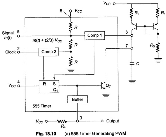
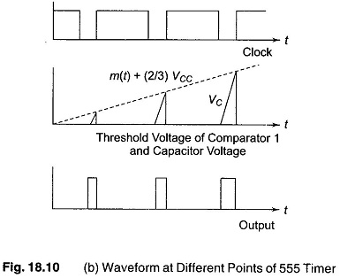
When Pin 2 is high, comparator 2 sets the output Q1 of the F/F high. This, in turn, turns QT ON and moves the buffer output to low. When a negative going clock pulse is applied to Pin 2, the output of F/F resets low. QT is cut off and C begins to charge linearly, as illustrated in Fig. 18.10(b). The buffer output remains high until the capacitor voltage, which appears at Pin 6, the input to comparator 1, reaches the value of the signal voltage which is applied to Pin 5 (input of comparator 1). This trips the output of comparator 1 and sets the F/F output high, the buffer output goes low and the capacitor rapidly discharges through QT. This cycle repeats upon application at the next pulse.
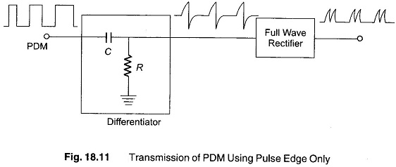
One method of transmitting PDMs more efficiently is to transmit only the pulse signals. Figure 18.11 shows the arrangement and the waveforms. At the receiving end, the appropriate pulse can be stretched to recover the original pulse.
Pulse Width Modulation demodulation is a simple process. The result is fed to an integrating circuit from which a signal output is obtained, whose amplitude at any time is proportional to the pulse width at that time.
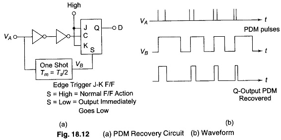
The circuit of Fig. 18.12 shows a PDM recovery circuit. It is assumed that the maximum duration of PDM is less than one third the signal period Ts. The one shot will set the F/F to zero only when two successive PDM pulses pass through with separations greater than Ts/3. This assumes that pulse 2 triggers the F/F to zero and that the next pulse that triggers the F/F corresponds to the leading edge of the transmitted pulse.
In demodulating PDM, the best results are obtained when it is converted to PAM and low pass filtered. A general block diagram of a PDM or PAM is shown in Fig. 18.13.
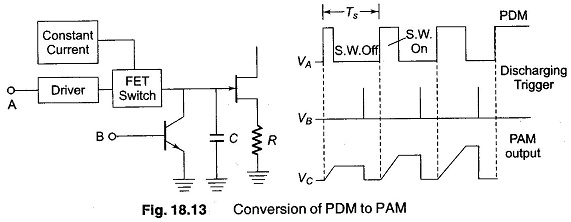
The constant current generator assures a linear voltage rise on the capacitor. Note that the discharging pulses have to be located beyond the widest pulse width. The easiest way to obtain such pulses is to produce narrow pulses by triggering a multivibrator and delaying it with another monostable.
PPM is very closely allied with PDM. In fact, it can be derived directly from PDM, as shown in Fig. 18.14.
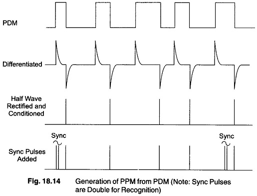
The PDM is differentiated, and then rectified and shaped. Remember that in PDM, it is the position of the pulse edges that carry the information and not the pulse itself. Therefore, PPM carries exactly the same information as long as the position of the clock pulses (leading edge) is well defined in the received signal.
It is easy to see that PPM is superior to PDM for message transmission, since the wide pulses of PDM require more energy than PPM when transmitted. Specifically, PPM is suited for communication in the presence of noise. Very high peak narrow pulses can be transmitted and the pulse position can be determined even when the noise level is high. Note however that transmitting very narrow pulses requires a large band width.
When light is used as the media for transmitting analog signals, PPM or PCM are the most suitable types of modulation because the maximum power output in the modulated light source, such as LED or LASER is achieved when it is pulsed at a very low duty cycle.
In transmitting PPM, it is necessary to transmit a series of sync pulses at a much lower repetition rate than the sampling pulses, so that they do not interfere with the original signal and/or minimise the number of pulses transmitted in order to conserve transmission power. In PPM, a series of double pulses are used for synchronisation, since the sync pulses must be narrow and at the same time distinguishable from the signal pulse.