Ideal Operational Amplifier:
The Ideal Operational Amplifier is basically an amplifier which amplifies the difference between the two input signals. In its basic form, the Op Amp is nothing but a differential amplifier. To understand the Ideal Characteristics of Operational Amplifier, let us discuss the operation of an ideal differential amplifier which is a basic building block of an op-amp.
Ideal Differential Amplifier:
The differential amplifier amplifies the difference between two input voltage signals. Hence it is also called difference amplifier.
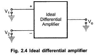
Consider an ideal differential amplifier shown in the Above Fig. 2.4. V1 and V2 are the two input signals while Vo is the single ended output. Each signal is measured with respect to the ground. In an ideal differential amplifier, the output voltage Vo is proportional to the difference between the two input signals. Hence we can write,
Differential Gain Ad:
From the equation (1) we can write,![]()
where Ad is the constant of proportionality. The Ad is the gain with which differential amplifier amplifies the difference between two input signals. Hence it is called differential gain of the differential amplifier.
Thus,
Ad = differential gain
The difference between the two inputs (V1 — V2) is generally called difference voltage and denoted as Vd.
Hence the differential gain can be expressed as,
Generally the differential gain is expressed in its decibel (dB) value as,
Common Mode Gain Ac:
If we apply two input voltages which are equal in all the respects to the differential amplifier i.e. V1 = V2 then ideally the output voltage Vo = (V1 – V2)Ad, must be zero. But the output voltage of the practical differential amplifier not only depends on the difference voltage but also depends on the average common level of the two inputs. Such an average level of the two input signals is called common mode signal denoted as Vc.![]()
Practically, the differential amplifier produces the output voltage proportional to such common mode signal, also. The gain with which it amplifies the common mode signal to produce the output is called common mode gain of the differential amplifier denoted as Ac.
Thus there exists some finite output for V1 = V2 due to such common mode gain Ac, in case of practical differential amplifiers. So the total output of any differential amplifier can be expressed as,
This shows that if one input is + 25 μV and other is – 25 μV then the output of the amplifier will not be same, with the inputs as 600 μV and 650 μV, though the difference between the two sets of the inputs is 50 μV.
For an ideal differential amplifier, the differential gain Ad must be infinite while the common mode gain must be zero. This ensures zero output for V1 = V2. But due to mismatch in the internal circuitry, there is some output available for V1 = V2 and gain Ac is not practically zero. The value of such common mode gain Ac is very very small while the value of the differential gain Ad is always very large. At this stage, we can define one important parameter of the differential amplifier known as common mode rejection ratio (CMRR).
Common Mode Rejection Ratio (CMRR):
When the same voltage is applied to both the inputs, the differential amplifier is said to be operated in a common mode configuration. Many disturbance signals, noise signals appear as a common input signal to both the input terminals of the differential amplifier. Such a common signal should be rejected by the differential amplifier.
The ability of a differential amplifier to reject a common mode signal is expressed by a ratio called common mode rejection ratio denoted as CMRR or ρ.
It is defined as the ratio of the differential voltage gain Ad to common mode voltage gain Ac.
Ideally the common mode voltage gain is zero, hence the ideal value of CMRR is infinite. For a practical differential amplifier Ad is large and Ac is small hence the value of CMRR is also very large.
Many a times, CMRR is also expressed in dB, as
Ideal Characteristics of Operational Amplifier:
With the background of an ideal differential amplifier and CMRR, let us study the ideal op-amp characteristics.
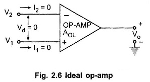
The Fig. 2.6 Above shows an ideal op-amp. It has two input signals V1 and V2 applied to non-inverting and inverting terminals, respectively.
The following things can be observed for the ideal op-amp shown in the Fig. 2.6.
- An ideal op-amp draws no current at both the input terminals i.e. I1 = I2 =0. Thus its input impedance is infinite. Any source can drive it and there is no loading on the driver stage.
- The gain of an ideal op-amp is infinite (∞), hence the differential input Vd = V1 – V2 is essentially zero for the finite output voltage Vo.
- The output voltage Vo is independent of the current drawn from the output terminals. Thus its output impedance is zero and hence output can drive an infinite number of other circuits.
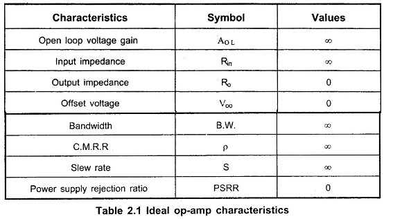
These properties are expressed generally as the characteristics of an ideal op-amp. The various characteristics of an ideal op-amp are :
Infinite voltage gain : It is denoted as AOL. It is the differential open loop gain and is infinite for an ideal Op Amp.
Infinite input impedance : The input impedance is denoted as Rin and is infinite for an ideal Op Amp. This ensures that no current can flow into an ideal op-amp.
Zero output impedance: The output impedance is denoted as Ro and is zero for an ideal Op Amp. This ensures that the output voltage of the op-amp remains same, irrespective of the value of the load resistance connected
Zero offset voltage : The presence of the small output voltage though V1 = V2 = 0 is called an offset voltage. It is zero for an ideal op-amp. This ensures zero output for zero input signal voltage.
Infinite bandwidth : The range of frequency over which the amplifier performance is satisfactory is called its bandwidth. The bandwidth of an ideal op-amp is infinite. This means the operating frequency range is from 0 to ∞. This ensures that the gain of the op-amp will be constant over the frequency range from d.c. (zero frequency) to infinite frequency. So op-amp can amplify d.c. as well as a.c. signals.
Infinite CMRR : The ratio of differential gain and common mode gain is defined as CMRR. Thus infinite CMRR of an ideal op-amp ensures zero common mode gain. Due to this common mode noise output voltage is zero for an ideal op-amp.
Infinite slew rate : This ensures that the changes in the output voltage occur simultaneously with the changes in the input voltage.
The slew rate is important parameter of Ideal Operational Amplifier. When the input voltage applied is step type which changes instantaneously then the output also must change rapidly as input changes. If output does not change with the same rate as input then there occurs distortion in the output. Such a distortion is not desirable. Infinite slew rate indicates that output changes simultaneously with the changes in the input voltage.
The parameter slew rate is actually defined as the maximum rate of change of output voltage with time and expressed as in V/μs.
Its ideal value is infinite for the Op Amp.
No effect of temperature : The characteristics of Ideal Operational Amplifier do not change with temperature.
Power Supply Rejection Ratio (PSRR) : The power supply rejection ratio is defined as the ratio of the change in input off set voltage due to the change in supply voltage producing it, keeping other power supply voltage constant. It is also called power supply sensitivity.
So if VEE is constant and due to change in VCC, there is change in input offset voltage then PSRR is expressed as
For a fixed VCC, if there is change in VEE causing change in input offset voltage then,
It is expressed in mV/V or μV/V and its ideal value is zero.
These ideal characteristics of op-amp are summarized in the Table Below 2.1


