Clamping Circuit:
Negative and Positive Voltage Clamping Circuits – A clamping circuit, also known as a dc restorer, changes the dc voltage level of a waveform, but does not affect its shape Consider the clamping circuit shown in Fig. 3-33.
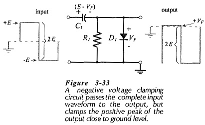
When the square wave input is positive, diode D1 is forward biased, and voltage equals the diode forward voltage drop (VF).
![]()
During the positive half-cycle of the input, the voltage side of the capacitor is +VF, while that on the left side +E. Thus, C1 is charged with the polarity shown to a voltage,
![]()
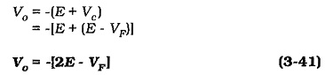
When the input goes negative, the diode is reverse biased and has no further effect on the capacitor voltage. Also, R1 has a very high resistance, so that it cannot discharge C1 significantly during the negative portion of the input waveform. While the input is negative, the output voltage is the sum of the input and capacitor voltages. Since the polarity of the capacitor voltage is the same as the (negative) input, the output is,
The peak-to-peak output voltage (Vo(PP)) is the difference between the positive output peak (VF) and negative output peak -(2E – VF).
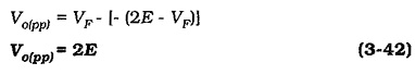
It is seen that the peak-to-peak amplitude of the output waveform from the clamping circuit is exactly the same as the peak-to-peak input. Instead of the waveform being symmetrical above and below ground, however, the output positive peak is clamped at a level of +VF.
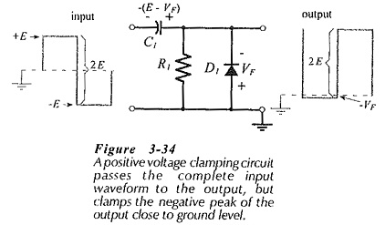
The circuit in Fig. 3-33 is known as a negative voltage clamping circuit, because the output waveform is almost completely negative. Reversing the polarity of the diode and capacitor in Fig. 3-33 creates the positive voltage clamping circuit shown in Fig. 3-34. As illustrated, the output waveform is clamped to keep it almost completely positive.
Output Slope:
Resistor R1 in Figs. 3-33 and 3-34 is sometimes termed a bleeder resistor. Its function is to gradually discharge the capacitor over several cycles of input waveform, so that it can be charged to a new voltage level if the input changes. However, R1 partially discharges the capacitor during the time that D1 is reverse biased, and this produces a slope, or tilt (ΔVc) on the output waveform, as illustrated in Fig. 3-35.
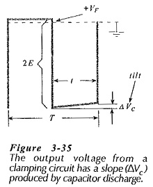
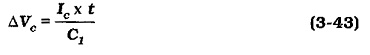
The tilt voltage can be calculated from a knowledge of the waveform frequency and the circuit component values. The constant-current equation for charging or discharging a capacitor may be applied,
Component Determination:
When designing a clamping circuit, capacitor C1 is selected so that it becomes completely charged in approximately five cycles of the input waveform. As already discussed (and illustrated in Fig. 3-37), diode D1 is forward biased when C1 is being charged.
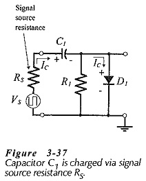
Resistor R1 is not part of the C1 charging circuit, because D1 bypasses R1. As illustrated, C1 charge is controlled by the signal source resistance (RS). A capacitor is completely charged in approximately five time constants of the circuit. In the case of a resistor-capacitor circuit, the time constant is RC. So, the charging time is,
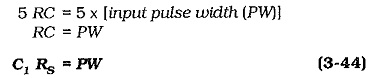
When the pulse width and source resistance of the input waveform is known, C1 can be determined from Eq. 3-44.
So long as the slope on the output waveform is very small, the capacitor discharge current is essentially a constant quantity.
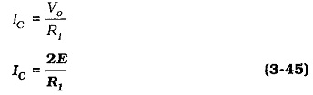
When the output waveform slope is specified, IC can be calculated from Eq. 3-43, and a suitable resistance for R1 is then determined by substituting IC into Eq. 3-45.
Biased Clamping Circuit:
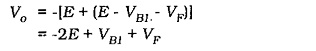
The biased clamping circuit shown in Fig. 3-39 has a bias voltage (VB) at the cathode of diode D1.
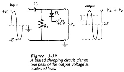
In this case, the output voltage cannot exceed (VB1 + VF), as illustrated. The capacitor charges to (E – VB1 – VF) when the input is positive. When the input goes negative, the output voltage is -(E + VC), giving,
The peak-to-peak output voltage is the difference between the positive and negative output peak levels.
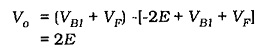
It is seen that, as for other clamping circuits, the peak-to-peak output waveform from the biased damper is the same as the input. The positive level of the output is clamped to (VB + VF).
Virtually any bias voltage level (positive or negative) can be used with a biased clamping circuit. The diode polarity determines whether the positive or the negative peak of the output is clamped. Care must be taken to ensure that the capacitor is connected with the correct polarity. Biased clamping circuits are designed in exactly the same way as unbiased clamping circuits.
Zener Diode Clamping Circuit:
Zener diode clamping circuits operate just like biased voltage dampers, with the Zener diode voltage (VZ) substituting for the bias voltage.
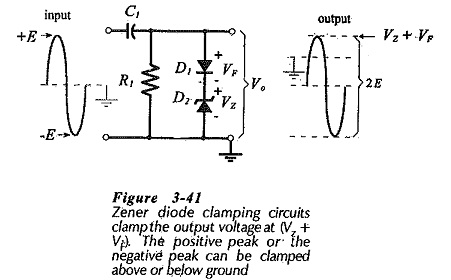
The circuit in Fig. 3-41 has an ordinary diode (D1) connected in series with a Zener diode (D2). When the input voltage is at its positive peak, the output voltage is,![]()
and C1 charges (+ on the left) to,
![]()
When the input goes to its negative peak, the output voltage is,
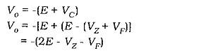
The peak-to-peak output remains equal to the peak-to-peak input voltage (2E). If the polarity of the diodes (and the capacitor) are reversed, the negative output peak is clamped at -(VZ + VF).