Solid State Modulator/Demodulator Circuit:
A solid state modulator/demodulator circuit is shown in Fig. 14.41. The transformer T is driven by an ac source and couples each secondary connected to the two transistor pairs, Q1 – Q2 and Q3 – Q4.
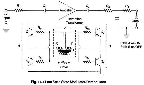
During the first half cycle, point X is positive with respect to point Y. This forward biases transistors Q1 – Q2 which are driven in full conduction. The resistance of the transistors falls. The current flow through the path is shown in Fig. 14.41 (arrow A). The other transistor Q3 – Q4 is reverse biased and its resistance increases. Therefore the output voltage increases.
During the second half cycle, the polarity reverses. making Y positive with respect to X; now transistor Q3 – Q4 conducts fully, reducing its resistance, and output. Transistor Q1 – Q2 are reverse biased. Its resistance increases, hence the output developed across it increases. Thus, it is seen that Q1 – Q2 act as a modulator which feeds an ac signal to the ac amplifier and Q3 – Q4 act as a demodulator, which demodulates the amplified ac signal to obtain dc again. The dc output obtained is an amplified value of the dc input.