Transistor Use in Static Relay:
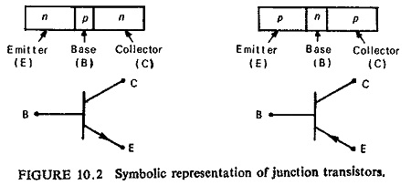
Transistor Use in Static Relay – In its simplest form, it consists of two pn junction diodes coupled together by a very thin common base, either of p-type or n-type semiconductor material. It is possible to separate input and output circuits, which may be controlling circuit and controlled circuit respectively. It has many advantages like small size, ruggedness, absence of filament heating power, etc., as compared to vacuum tubes. Another main advantage of transistors is that it can be made in two types; pnp transistor in which a region of n-type is sandwiched between two regions of p-type and vice versa in npntype. The symbolic representation and the nomenclature of Transistor Use in Static Relay are shown in Fig. (10.2).
Two factors are important in relation to transistor characteristics; one is the collector-emitter amplification factor (α) which is defined as the negative of the ratio of a change in collector current Δic to a given change in emitter current Δie, with collector-to-emitter voltage held constant, i.e.
![]()
The other important factor is current amplification factor (β) which is the ratio of a change in collector cu rent Δie to a given change bias current Δib, with collector-to-base voltage held constant, i.e.
![]()
The value of α lies between 0.95 to 0.99 and β may reach values as high as several hundred.
The common-emitter configuration or grounded-emitter configuration is usually employed in most of the transistors. Figure (10.3) shows such a configuration.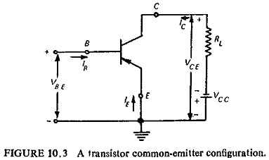
The base-emitter terminals are often employed as the controlling terminals, whereas the collector-emitter terminals are the controlled terminals.
The input current and the output voltage are taken as the independent variables, whereas the input voltage and output current are the dependent variables. Therefore, we have
![]()
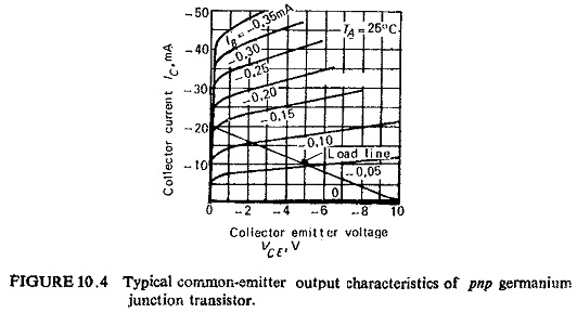
Equation (10.7) describes the family of input characteristic curves, and Eq. (10.8) describes the family of output characteristic curves. Typical output and input characteristic curves for pnp junction, germanium transistor are given in Fig. (10.4) and (10.5) respectively.
![]()
The idealized collector characteristics shown in Fig. (10.6) have three regions of operation. Region I where virtually zero collector current flows and the base current IB ≤ 0, this is also known as cut off region. It is not enough to reduce IB to zero for cut off, instead it is necessary to reverse-bias the emitter junction slightly. In region II the collector current is a linear function of base current, this is the active region of operation. In the active region the collector junction is reverse biased and the emitter junction is forward biased.
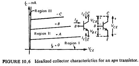
In this region the transistor output current responds most sensitively to an input signal. If the transistor is to be used as an amplifying device without appreciable distortion, it must be restricted to operate in this region. In region III which is the saturated region the collector junction (as well as the emitter junction) is forward biased by at least the cut in voltage. VCE is only a few tenths of a volt at saturation. Hence in Fig. (10.6) the saturation region is very close to the zero voltage axis where all the curves merge and fall rapidly toward the origin.
Transistor as a Switch:
The switching capabilities of a transistor stem from the capability of the device to rapidly change the d.c. resistance between its output terminals, the collector and emitter, from a very high to a very low value, in response to a small current injected into the control (base) terminal.
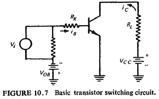
A schematic of a basic transistor switching circuit is shown in Fig. (10.7). A voltage pulse (Vi) applied to the input terminal causes a current flow (iB) through the base resistance (RK) which in turn reduces the collector-emitter resistance to a very low value and permits a large current flow (iC) from the battery through the load. The transistor gets saturated and operates in region III. If the input voltage is removed, the reverse bias voltage (VOB) causes the collector-emitter resistance to increase greatly, and significantly reduces the load current.
Transistor Use in Static Relay, though they fall short of perfection represent the best available components for switching applications, especially in high-speed equipment. Factors that prevent a transistor from duplicating an ideal switch are:
- A residual leakage current when the transistor is off.
- A residual collector-emitter saturation voltage when the transistor is on.
- Time delays involved in the response of collector current to changes in the input signal.
Transistor Amplifiers:
There are three basic methods of connection of a transistor in an amplifier circuit. Figure (10.8) shows these connections for both pnp and npn transistors. The emitter-base junction is always forward biased and the collector-base junction is always reverse biased. By sending a current through the emitter-base junction at a low voltage, almost the same amount of current is made to flow in the comparatively high voltage collector circuit. This accounts for the power amplification achieved. Because of its high gain, the common emitter circuit is most commonly used.
![]()
The fact that current amplification is linear, whereas the voltage amplification depends upon the load impedance, means that transistor amplifiers are linear only as current amplifiers, i.e. the input must be a current source or the source impedance must be high compared with the transistor input impedance if a voltage source is used.
Table 10.1 gives in short the various features of the three different amplifier connections.
![]()
D.C. Amplifiers:
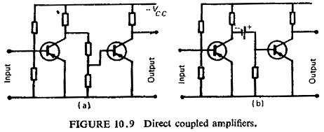
These are amplifiers which have zero frequency as the lower band limit to retain the initial displacements, d.c. components and low-frequency transient offsets that may accompany the a.c. and time-varying signals. It is not possible to use reactive coupling elements to separate signals and bias quantities. Any drift in the quiescent operating values cannot be distinguished from signals which are to be amplified. Direct-coupled amplifiers, therefore, have special problems in long-time stability. The main reasons for the drift are (i) variation of emitter-to-base voltage, (ii) variation in the gain of the transistor and (iii) variation in the power supply voltage. Temperature variation is one of the main causes of these variations. Numerous compensation techniques and circuits have been developed and are in use.
Two principal schemes of direct-coupled amplifiers are shown in Fig. (10.9). The only difference between the two schemes is that the resistance potential divider of Fig. (10.9a) is replaced by a battery in series with a resistance in Fig. (10.9b).
An alternative method is to use a chopper which converts a slowly varying direct current to an alternating form, which is amplified by an a.c. amplifier, and its output is either used in a.c. form or rectified back to direct current again.
Typical transistor chopper circuits are shown in Fig. (10.10). The circuit shown in Fig. (10.10a) is suited for general use. When the base is driven positive by the square-wave output of the driving transformer, the transistor closes the circuit and the d.c. input voltage appears across R2. When the base is driven negative, the transistor is switched open and the voltage across R2 is zero. The circuit of Fig. (10.10b) uses two transistors, and it is useful with low-resistance sources since it has an on-off switch in series and an off-on switch in shunt with the source. When TA is on, the collector-to-base junction of TB is reverse-biased; and for the succeeding half cycle of switching frequency, when TB is on, the junction of TA is reverse-biased.
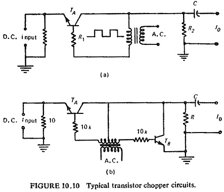
The leakage current of TA is shorted out of the load by TB during the half cycle in which TA is open, and leakage current of TB passes largely through TA on the reverse half cycle, if R is large. The offset or threshold voltages of both transistors are identically applied across R on successive half cycles, but this voltage does not reverse and thus acts as a d.c. component which is removed by C.