Unijunction Transistor in Static Relay:
Unijunction Transistor in Static Relay is a three terminal device with only one pn-junction. It is made up of n-type silicon wafer having two base controls and a p-type alloy junction which acts as emitter electrode.
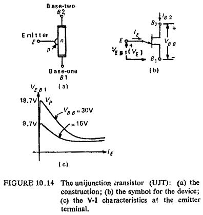
In normal operation the lower ohmic contact (base B1) is grounded. If the emitter junction is left open circuited, the voltage between B1 and B2 sets up a current proportional to the conductance of the wafer. The base B2 is made positive with respect to B1 by voltage VBB and a fraction η of this voltage appears between the emitter E and B1. Under the conditions of no current in the emitter, the UJT between B1 and B2 has the characteristics of an ordinary resistance called the interbase resistance RBB. At 25°C this resistance lies between 4 and 10 kΩ, and increases linearly with temperature up to about 140°C.
The normal biasing conditions for the Unijunction Transistor in Static Relay and its symbol are indicated in Fig. (10.14). 
If VE applied is less than ηVBB, the emitter will be reverse biased and only leakage current will flow. If VE is greater than ηVBB the junction becomes forward biased and large emitter current flows with a low forward voltage drop between emitter and B1.
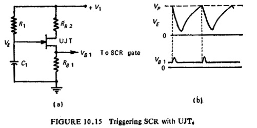
The characteristics show that there is a large negative resistance region for fast switching action. The use of UJT is in generating trigger input to SCRs. For such an application, the basic circuit of Fig. (10.15) is used.
The capacitor C1 charges through R1 until VE reaches the peak-point voltage VP, when the UJT triggers and discharges C1 through RB1. When VE reaches a low value, perhaps 2V, the capacitor can no longer supply the necessary emitter-base current, and UJT turns off. Base resistor RB1 provides an output-voltage pulse during the very short high-current transition through the negative resistance region as shown in Fig. (10.15b). This pulse is coupled to the gate of an associated SCR and provides precise triggering.
